Automatic focus and emissivity measurements for a substrate system

Inactive Publication Date: 2009-08-13
APPLIED MATERIALS INC
View PDF15 Cites 49 Cited by
  • Summary
  • Abstract
  • Description
  • Claims
  • Application Information

AI Technical Summary

Benefits of technology

[0017]In another aspect, embodiments of the invention relate to a method of thermally processing a substrate. The method includes directing radiation at a first wavelength from a heating radiation source onto a substrate and directing radiation at a second wavelength from a low power radiation source onto the substrate. A focus plane of the low power radiat

Problems solved by technology

While such processes are widely used, current technology tends to ramp the temperature of the substrate too slowly and expose the substrate to elevated temperatures for too long.
These problems become more severe with increasing substrate sizes, increasing switching speeds, and/or decreasing feature sizes.
A drawback of RTP is that it heats the entire substrate even though the integrated circuit (IC) devices reside only in the top few microns of the silicon substrate, which limits how fast one can heat up and cool down the substrate.
Moreover, once the entire substrate is at an elevated temperature, heat can only dissipate into the surrounding space or structures.
As a result, today's state of the art RTP systems struggle to achieve a 400° C./s ramp-up rate and a 150° C./s ramp-down rate.
A drawback of RTP is that it heats the entire substrate even though the IC devices reside only in the top few microns of the substrate.
The heating of the entire substrate limits how fast one can heat up and cool do

Method used


Image

  • Automatic focus and emissivity measurements for a substrate system
  • Automatic focus and emissivity measurements for a substrate system
  • Automatic focus and emissivity measurements for a substrate system

Examples


Embodiment Construction

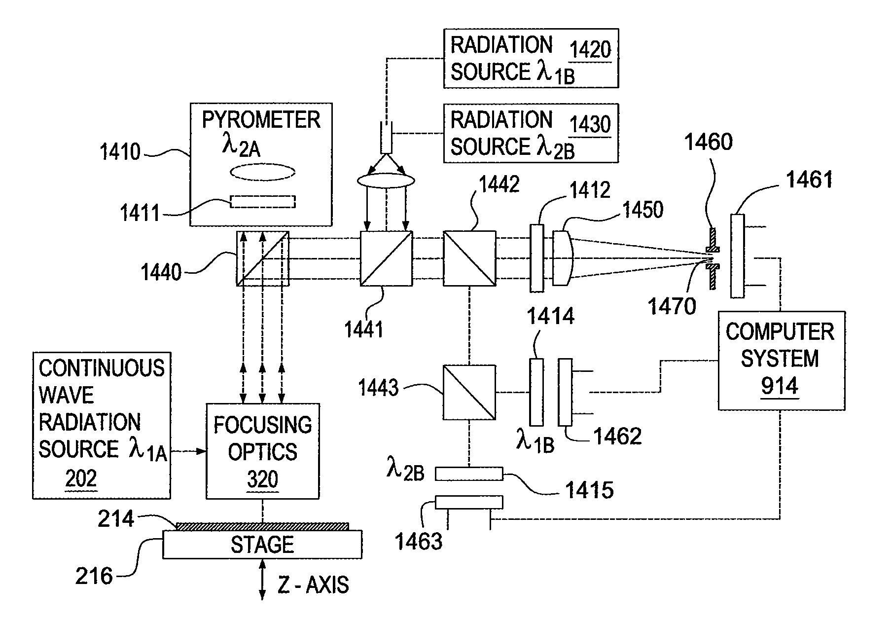
[0038]Embodiments of the invention generally relate to thermal processing of substrates, and, more specifically, to apparatus and methods for automatically focusing radiation onto a substrate during thermal processing.

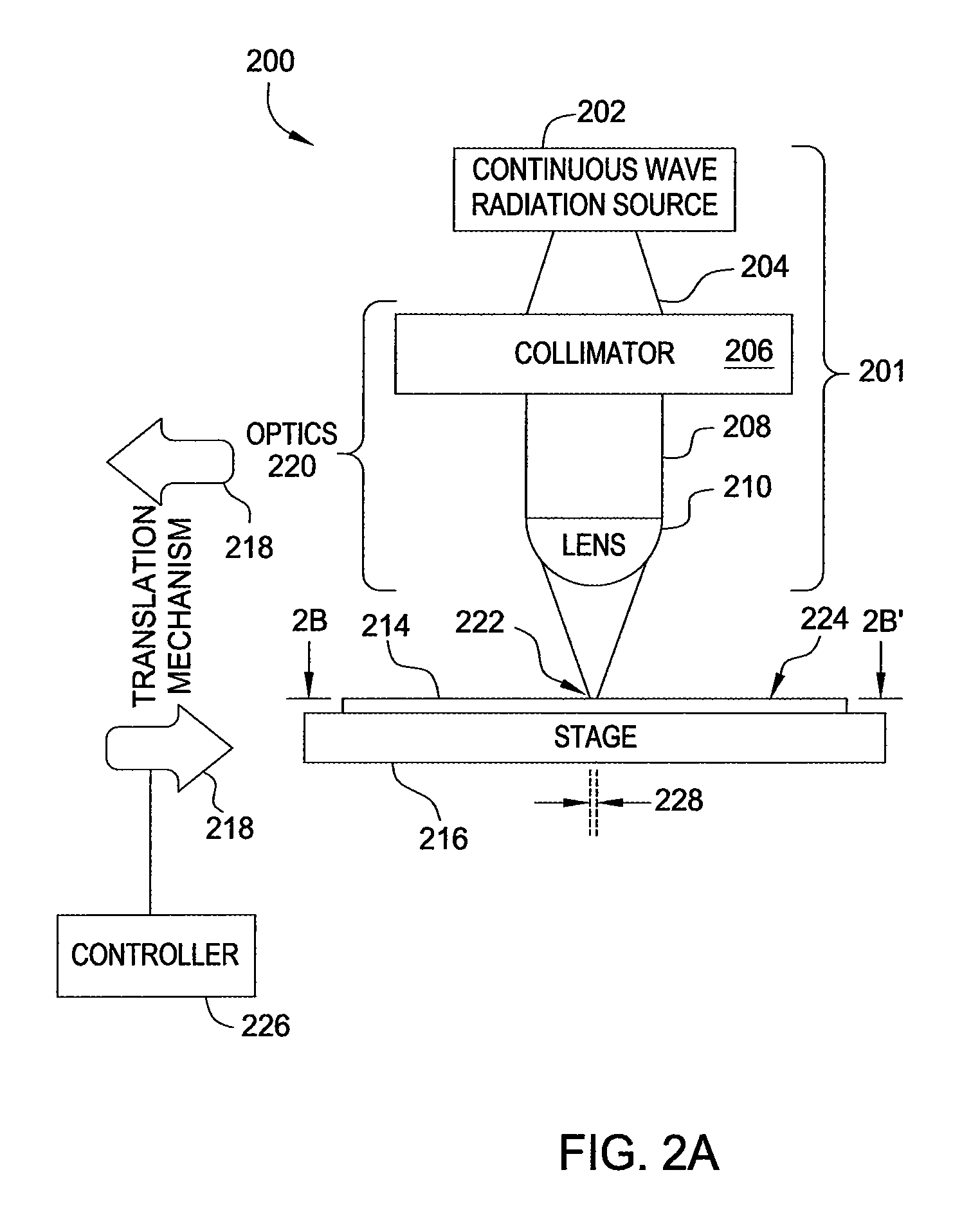
[0039]FIG. 2A is a side view of an apparatus 200 for thermally processing a substrate, according to an embodiment of the invention. Thermally processing a substrate means conducting any thermal process that requires the characteristics of the invention described below. Embodiments of such a thermal process may include thermal annealing of substrates or thermal processes used in chemical vapor deposition (CVD), both of which will be described throughout the remainder of the figures.

[0040]The apparatus 200 comprises a continuous wave electromagnetic radiation module 201, a stage 216 configured to receive a substrate 214 thereon, and a translation mechanism 218. The continuous wave electromagnetic radiation module 201 comprises a continuous wave electromagnetic radiation ...


PUM

PropertyMeasurementUnit
Nanoscale particle sizeaaaaaaaaaa
Wavelengthaaaaaaaaaa
Temperatureaaaaaaaaaa

Abstract

An apparatus for thermally processing a substrate includes a first radiation source configured to heat a substrate and emit radiation at a heating wavelength, focusing optics configured to direct radiation from the first radiation source to the substrate, and a second radiation source configured to emit radiation at a second wavelength different from the heating wavelength and at a lower power than the first radiation source. Radiation from the second radiation source is directed onto the substrate. The apparatus further includes a first detector configured to receive reflected radiation at the second wavelength and a computer system configured to receive an output from the first detector and adjust a focus plane of the first radiation source relative to the substrate. The second radiation source is configured to have substantially the same focus plane as the first radiation source.

Description

BACKGROUND OF THE INVENTION[0001]1. Field of the Invention[0002]Embodiments of the invention generally relate to thermal processing of substrates, and, more specifically, to apparatus and methods for automatically focusing energy onto and measuring emissivity of a substrate during thermal processing.[0003]2. Description of the Related Art[0004]During electronic device fabrication, substrates may be heated to high temperatures so that various chemical and / or physical reactions can take place. Thermal processes are usually used to heat the substrates. A typical thermal process, such as annealing, requires providing a relatively large amount of thermal energy to the substrate in a short amount of time, and thereafter rapidly cooling the substrate to terminate the thermal process. Examples of thermal processes currently in use include Rapid Thermal Processing (RTP) and impulse (spike) annealing. While such processes are widely used, current technology tends to ramp the temperature of th...

Claims


Application Information

Patent Timeline
IPC IPC(8): B23K26/04B23K26/06G01N21/55G01J5/02
CPCB23K26/0639B23K26/0613B23K26/0665B23K26/123G01J5/0003G01J5/0007G01J5/02G01J5/029G01J5/04G01J5/061G01J5/08G01J5/0803G01J5/0806G01J5/0821G01J5/0846G01J5/0896B23K26/03B23K26/032B23K26/034B23K26/046B23K26/0648B23K26/064G01J5/051
Inventor LI, JIPING
Owner APPLIED MATERIALS INC
Why Eureka
Try Eureka