Organic light emitting device and method of manufacturing the same

Active Publication Date: 2009-08-13
SAMSUNG DISPLAY CO LTD
View PDF4 Cites 61 Cited by
  • Summary
  • Abstract
  • Description
  • Claims
  • Application Information

AI Technical Summary

Benefits of technology

[0014]The present invention provides an OLED having improved color reproducibility, as well as a method of manufacturing the same.

Problems solved by technology

However, LCDs are disadvantageous as light emitting and receiving devices in that they require a backlight and have many limitations with regard to response speed and viewing angle.
However, as the size of the OLED increases, it becomes difficult to deposit the emission layer in each pixel using the fine shadow mask.
However, the color filters generally comprise limited color reproducibility, so the light that passes through the color filters may have color reproducibility that is the same as or lower than the color reproducibility of the color filters.
Thus, high color reproducibility, such as that required by the National Television Systems Committee (NTSC), may be difficult to achieve.

Method used


Image

  • Organic light emitting device and method of manufacturing the same
  • Organic light emitting device and method of manufacturing the same
  • Organic light emitting device and method of manufacturing the same

Examples


exemplary embodiment 1

[0033]An OLED according to one exemplary embodiment of the present invention will now be described in detail with reference to FIG. 1.

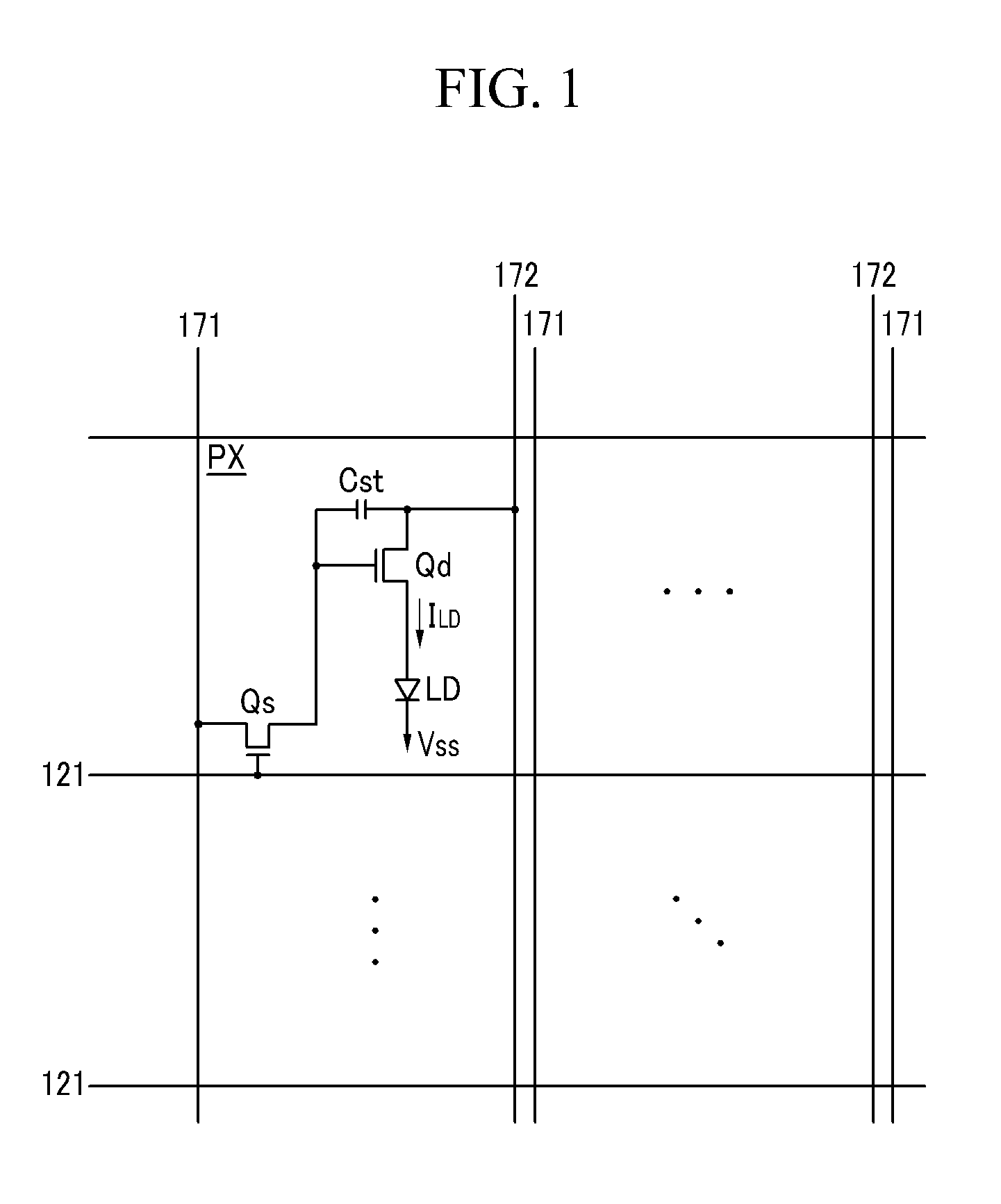
[0034]FIG. 1 is an equivalent circuit diagram of an OLED according to one exemplary embodiment of the present invention.

[0035]Referring to FIG. 1, the OLED includes a plurality of signal lines 121, 171, and 172 and a plurality of pixels PX connected to the signal lines 121, 171, and 172 and arranged in a matrix form.

[0036]The signal lines include a plurality of gate lines 121 that transfer gate signals (or scan signals), a plurality of data lines 171 that transfer data signals, and a plurality of driving voltage lines 172 that transfer driving voltages. The gate lines 121 extend in a row direction and are parallel to each other, and the data lines 171 and the driving voltage lines 172 extend in a column direction and are parallel to each other.

[0037]Each pixel PX includes a switching thin film transistor (TFT) Qs, a driving TFT Qd, a storage capacitor...

exemplary embodiment 2

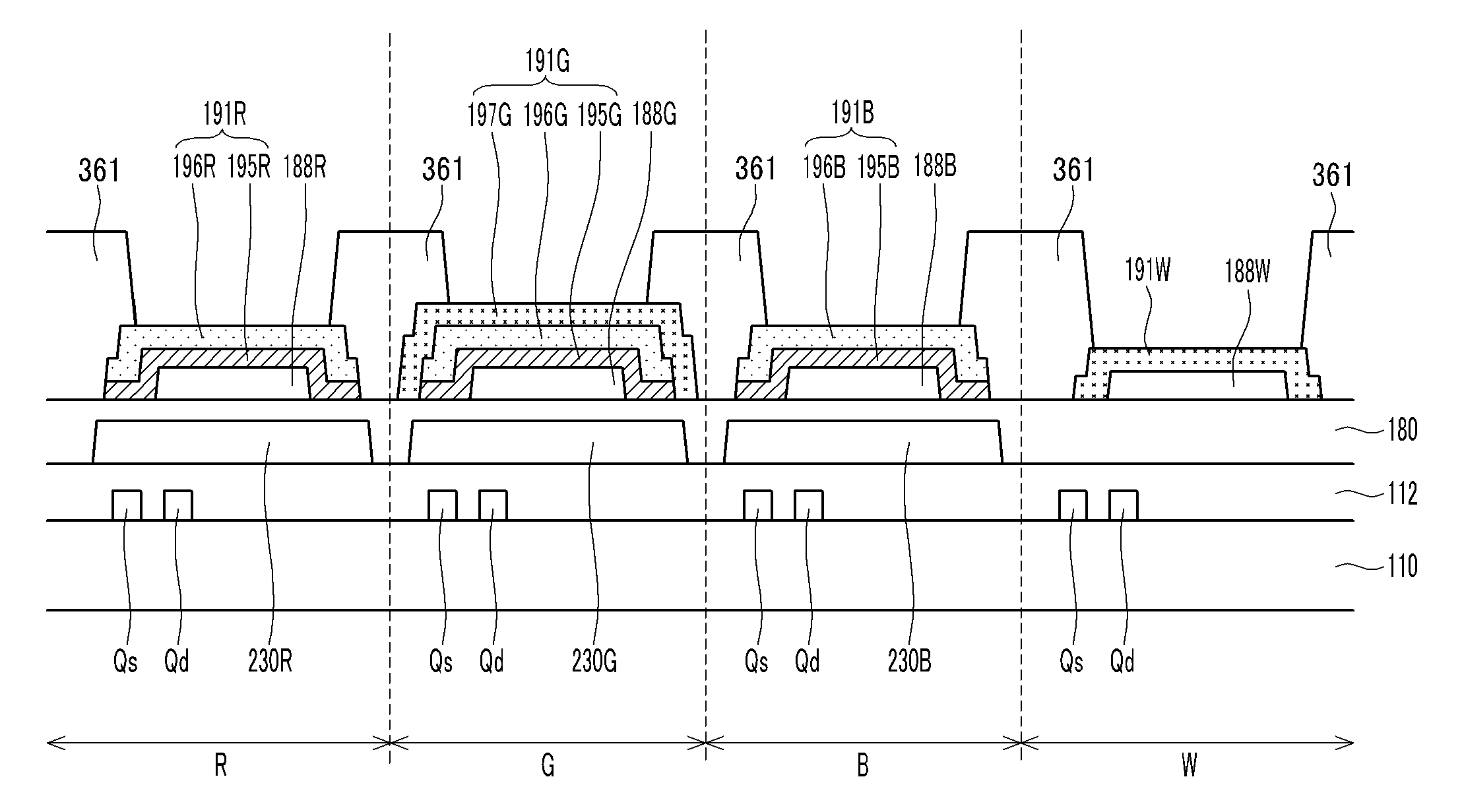
[0102]The OLED in FIG. 14, according to another exemplary embodiment of the present invention, will now be described with reference to FIG. 1 and FIG. 2.

[0103]FIG. 14 is a cross-sectional view showing the structure of an OLED according to another exemplary embodiment of the present invention.

[0104]A TFT array including switching TFTs Qs and driving TFTs Qd is arranged on the insulation substrate 110 in each pixel.

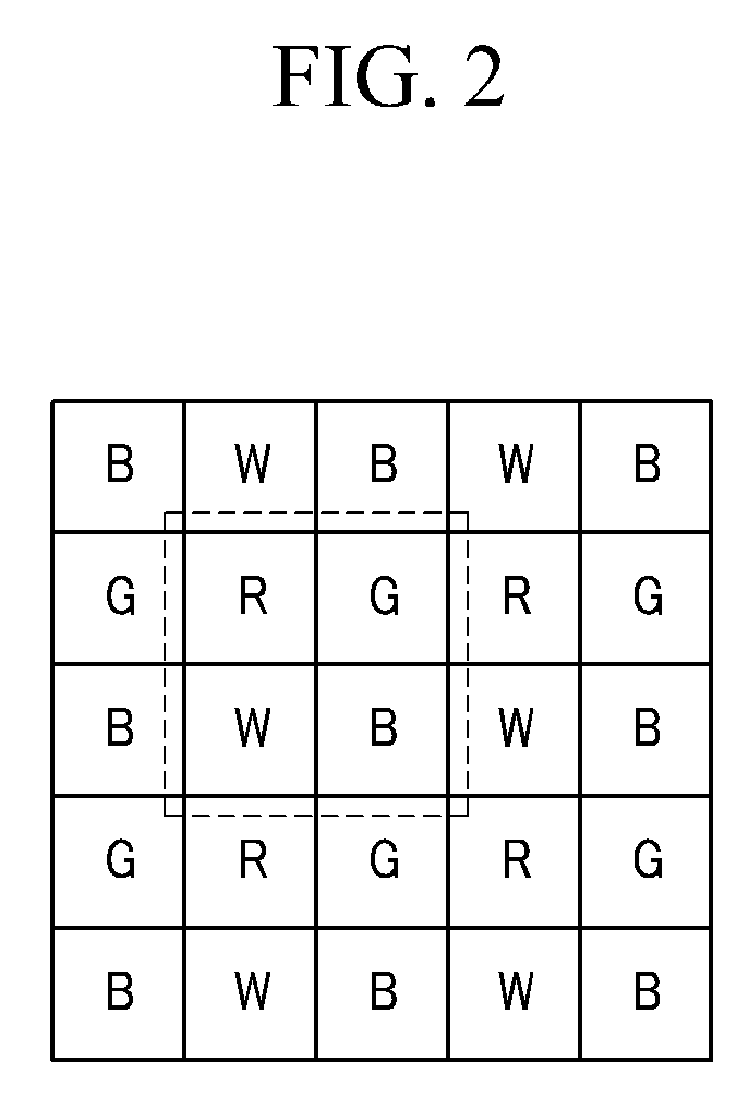
[0105]The passivation layer 112 is disposed on the TFT arrays, and red filters 230R, green filters 230G, and blue filters 230B are disposed on the passivation layer 112 at the red pixels R, the green pixels G, and the blue pixels B, respectively. Either no color filters or transparent white filters (not shown) may be formed in the white pixels W. The overcoat layer 180 is disposed on the color filters 230R, 230G, and 230B, and on the passivation layer 112.

[0106]The pixel electrodes 191R, 191G, 191B, and 191W are disposed on the overcoat layer 180.

[0107]Also, in this exempla...

exemplary embodiment 3

[0135]A further exemplary embodiment of the present invention will be described in detail with reference to FIG. 22 as well as FIG. 1 and FIG. 2.

[0136]FIG. 22 is a cross-sectional view showing the structure of an OLED according to another exemplary embodiment of the present invention.

[0137]Unlike the above-described exemplary embodiments, in this exemplary embodiment, an auxiliary layer is provided in each pixel to adjust the length of the microcavity.

[0138]A TFT array including a switching TFT Qs and a driving TFT Qd is arranged on the insulation substrate 110 in each pixel.

[0139]The passivation layer 112 is disposed on the TFT arrays, and the red filters 230R, the green filters 230G, and the blue filters 230B are disposed on the passivation layer 112 in the red pixels R, the green pixels G, and the blue pixels B, respectively. Either no color filters or transparent white filters (not shown) may be disposed in the white pixels W. The overcoat layer 180 is disposed on the color filt...


PUM


Abstract

An organic light emitting device includes first, second, and third pixels each displaying a different color. Each pixel includes a first electrode, a second electrode facing the first electrode, and an emission layer between the first and second electrodes. The first electrodes of the first and second pixels respectively include a first transparent conductive layer and a translucent conductive layer disposed on at least one of lower and upper portions of the first transparent conductive layer and forming microcavities together with the second electrodes, and the first electrode of the third pixel includes a second transparent conductive layer that is different from the first transparent conductive layer and a translucent conductive layer disposed on at least one of upper and lower portions of the second transparent conductive layer and forming a microcavity together with the second electrode.

Description

CROSS-REFERENCE TO RELATED APPLICATION[0001]This application claims priority from and the benefit of Korean Patent Application Nos. 10-2008-0012623 and 10-2008-0030437 filed on Feb. 12, 2008, and Apr. 1, 2008, respectively, which are hereby incorporated by reference for all purposes as if fully set forth herein.BACKGROUND OF THE INVENTION[0002]1. Field of the Invention[0003]The present invention relates to an organic light emitting device and a method of manufacturing the same.[0004]2. Discussion of the Background[0005]As the demand for lighter and thinner monitors and TVs increases, cathode ray tubes (CRTs) are being replaced by liquid crystal displays (LCDs).[0006]However, LCDs are disadvantageous as light emitting and receiving devices in that they require a backlight and have many limitations with regard to response speed and viewing angle.[0007]Recently, organic light emitting devices (OLEDs) have received much attention as display devices that can overcome such limitations.[00...

Claims


Application Information

Patent Timeline
IPC IPC(8): H01L51/52H01L21/28
CPCH01L27/3213H01L27/322H01L51/5265H01L27/3258H01L51/5215H01L27/3244H10K59/351H10K59/38H10K59/12H10K59/124H10K50/816H10K50/852
Inventor LEE, SUNG-SOOCHUNG, JIN-KOOKIM, SEONG-MINCHU, CHANG-WOONG
Owner SAMSUNG DISPLAY CO LTD
Why Eureka
Try Eureka