Field effect transistor

Active Publication Date: 2009-08-20
MURATA MFG CO LTD
View PDF12 Cites 15 Cited by
  • Summary
  • Abstract
  • Description
  • Claims
  • Application Information

AI Technical Summary

Benefits of technology

[0025]According to a further aspect, the dielectric film has a two-layered structure, and dielectric constant of a first dielectric film as an upper layer is higher than dielectric constant of a second dielectric film as a lower layer. Here, the balance between collapsing and gate breakdown voltage can be improved, and even if the surface state varies because of variation in manufacturing process, good performance of FET can stably be realized. Here, the second dielectric film may be interposed between the gate electrode and the surface layer of semiconductor substrate. FET adapted to be the MIS (Metal Insulator Semiconductor) type as described above is advantageous as the power transistor handling electric power, since switching speed increases and breakdown resistance is improved. The

Problems solved by technology

Therefore, these structures cannot be utilized for a high voltag

Method used


Image

  • Field effect transistor
  • Field effect transistor
  • Field effect transistor

Examples


Example

First Embodiment

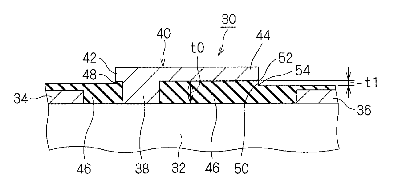
[0043]Referring to FIG. 1, an FET 30 in accordance with the first embodiment of the present invention is applied to a high voltage semiconductor device such as a high voltage switching element, and it includes a GaN epitaxial substrate 32, a source electrode 34, a drain electrode 36 and a gate electrode 38.

[0044]GaN epitaxial substrate 32 has a hetero junction structure including a buffer layer of GaN, an electron channel layer of undoped GaN, and an electron supplying layer of undoped AlGaN thinner than the electron channel layer, stacked successively on a semiconductor substrate such as a sapphire substrate. These buffer layer, electron channel layer and electron supplying layer are formed on the semiconductor substrate mentioned above, by an epitaxial growth method such as molecular beam epitaxy (MBE). In the present embodiment, the buffer layer, the electron channel layer and the electro supplying layer have the film thickness set to 20 nm, 2 nm and 25 nm. It is ...

Example

Second Embodiment

[0064]Referring to FIG. 4, an FET 230 in accordance with the second embodiment is characterized in that a recess 80 is formed at a portion of dielectric film 246 between source electrode 34 and a terminal end surface of a first visor portion 248 of field plate 40, and at a portion between drain electrode 36 and a terminal end surface of a second visor portion 250 of field plate 40, respectively. Except for this point, the structure is the same as that of the first embodiment.

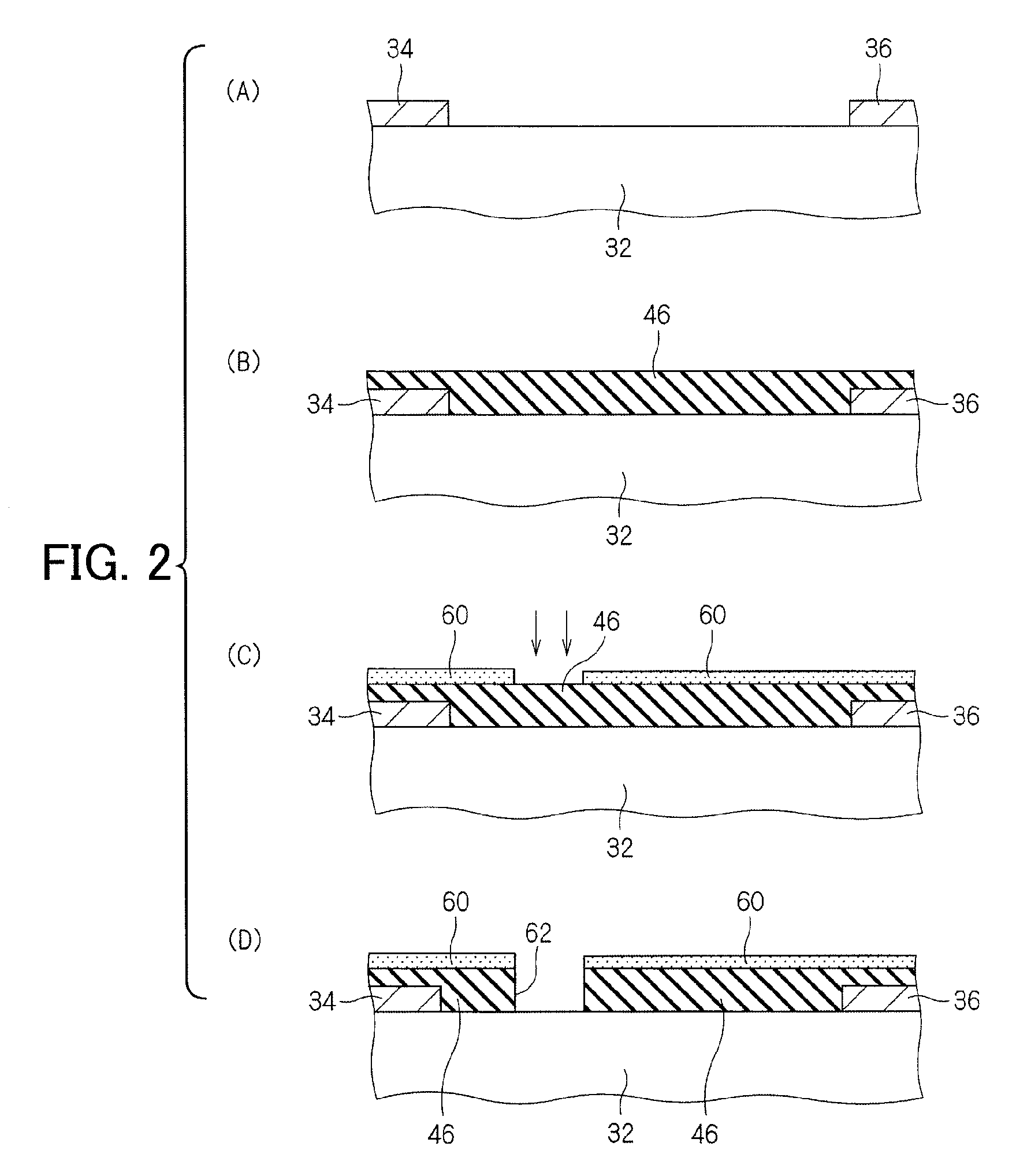
[0065]Referring to FIGS. 5 and 6, FET 230 is manufactured in the following manner. The process from the step of attaining ohmic contact of source electrode 34 and drain electrode 36 to the step of forming gate electrode 38 having field plate 40 shown in FIGS. 5(A) to 6(B) are the same as those of the first embodiment and, therefore, description of these process steps will not be repeated.

[0066]When formation of gate electrode 38 having the field plate structure ends, regions other than the reces...

Example

Third Embodiment

[0069]Referring to FIG. 7, an FET 330 in accordance with the third embodiment of the present invention is characterized in that dielectric film 346 has a two-layered structure including first and second dielectric films 100 and 102 having mutually different dielectric constants. Except for this point, the structure is the same as that of the first embodiment.

[0070]Dielectric constant of the first dielectric film 100 as the upper layer is set to be higher than that of the second dielectric film 102 as the lower layer. Specifically, the first dielectric film 100 is formed of TaOx, and the second dielectric film 102 is formed of SiNx. In the present embodiment, Ta2O5 is used as the first dielectric film 100, and SiN is used as the second dielectric film 102.

[0071]Referring to FIGS. 8 to 10, FET 330 in accordance with the present embodiment is manufactured in the following manner.

[0072]First, as shown in FIG. 8(A), by lift-off, source electrode 34 and drain electrode 36 ...


PUM


Abstract

A field effect transistor includes a GaN epitaxial substrate, a gate electrode formed on an electron channel layer of the substrate, and source and drain electrodes arranged spaced apart by a prescribed distance on opposite sides of the gate electrode. The source and drain electrodes are in ohmic contact with the substrate. At an upper portion of the gate electrode, a field plate is formed protruding like a visor to the side of drain electrode. Between the electron channel layer of the epitaxial substrate and the field plate, a dielectric film is formed. The dielectric film is partially removed at a region immediately below the field plate, to be flush with a terminal end surface of the field plate. The dielectric film extends from a lower end of the removed portion to the drain electrode, to be overlapped on the drain electrode.

Description

CROSS-REFERENCE TO RELATED APPLICATION[0001]This nonprovisional application claims priority under 35 U.S.C. § 119(a) on Patent Application No. 2008-000470 filed in Japan on Jan. 7, 2008, the entire contents of which are hereby incorporated by reference.BACKGROUND OF THE INVENTION[0002]1. Field of the Invention[0003]The present invention relates to a field effect transistor (hereinafter denoted as an “FET”) in which a prescribed electrode has a field-plate structure.[0004]2. Description of the Background Art[0005]As is well known, a nitride compound semiconductor material such as GaN, InGaN, AlGaN and AlInGaN has higher band gap energy than GaAs material and, hence, it has high breakdown voltage. Therefore, a device using a nitride compound semiconductor material is superior in operation under high voltage.[0006]Recently, application of an electronic device, particularly an FFT using GaN, to a high voltage semiconductor device such as a power supply device, has been considered promis...

Claims


Application Information

Patent Timeline
IPC IPC(8): H01L29/808
CPCH01L29/0692H01L29/2003H01L29/402H01L29/812H01L29/66462H01L29/66871H01L29/7787H01L29/42316
Inventor YAFUNE, NORIMASATWYNAM, JOHN KEVIN
Owner MURATA MFG CO LTD
Why Eureka
Try Eureka