Power switching circuit improved to reduce loss due to reverse recovery current

Active Publication Date: 2009-08-20
DENSO CORP
View PDF2 Cites 62 Cited by
  • Summary
  • Abstract
  • Description
  • Claims
  • Application Information

AI Technical Summary

Benefits of technology

[0019]Thus, as compared with the structure in which no second inductance is provided in the second commutation path or the second inductance is lower than the first inductance, it is possible to reduce a reverse recovery current through the first diode. This allows the sum of a current flowing through each of the first and second diodes after the commutation period to be immediately reduced. Note that, because the second diode has a reverse recovery characteristic superior than that of the first diode based on the difference between their reverse recovery times, an adverse effect of the reverse recovery characteristic of the second diode is relatively reduced.
[0020]In addition

Problems solved by technology

For this reason, when a PN junction diode is used to be connected in antiparallel to such a semiconductor switching element, during the reverse recovery time, the reverse recovery current flows through the diode, resulting in increasing switching loss and noise.
This results in increasing switching loss and noise.
However, when a MOSFET with the super junction structure (SJ) is used as a semiconductor switching element to be installed in a power converter, the reverse recovery current flowing through the intrinsic diode becomes high and has a steep time characteristic.
This resul

Method used


Image

  • Power switching circuit improved to reduce loss due to reverse recovery current
  • Power switching circuit improved to reduce loss due to reverse recovery current
  • Power switching circuit improved to reduce loss due to reverse recovery current

Examples


Example

[0038]an actually measured current that rises when the low-side MOSFET is ON in the power switching circuit according to the embodiment;

[0039]an actually measured current that rises when the low-side MOSFET is ON in a first comparative power switching circuit; and

[0040]an actually measured current that rises when the low-side MOSFET is ON in a second comparative power switching circuit.

DETAILED DESCRIPTION OF EMBODIMENTS OF THE INVENTION

[0041]An embodiment of the present invention will be described hereinafter with reference to the accompanying drawings.

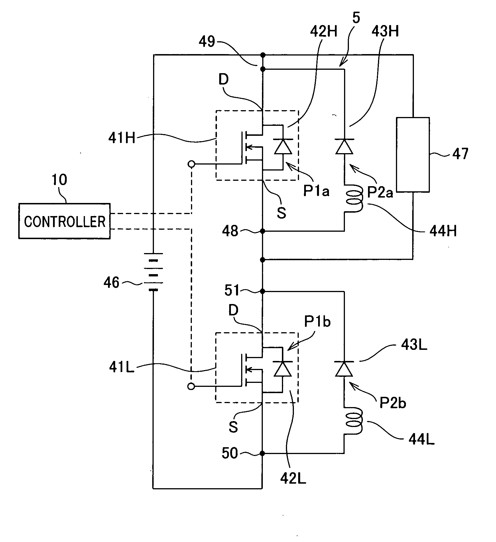
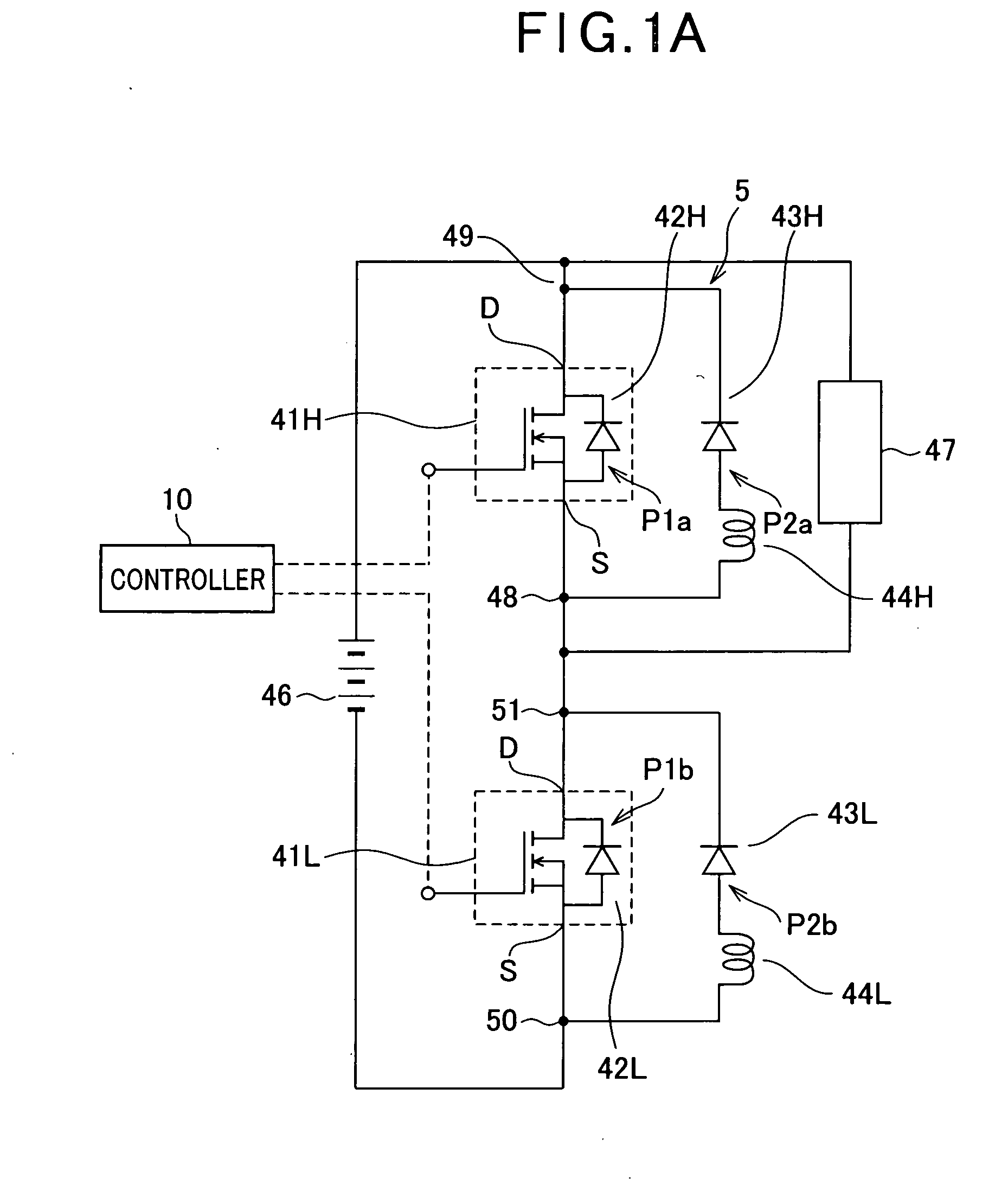
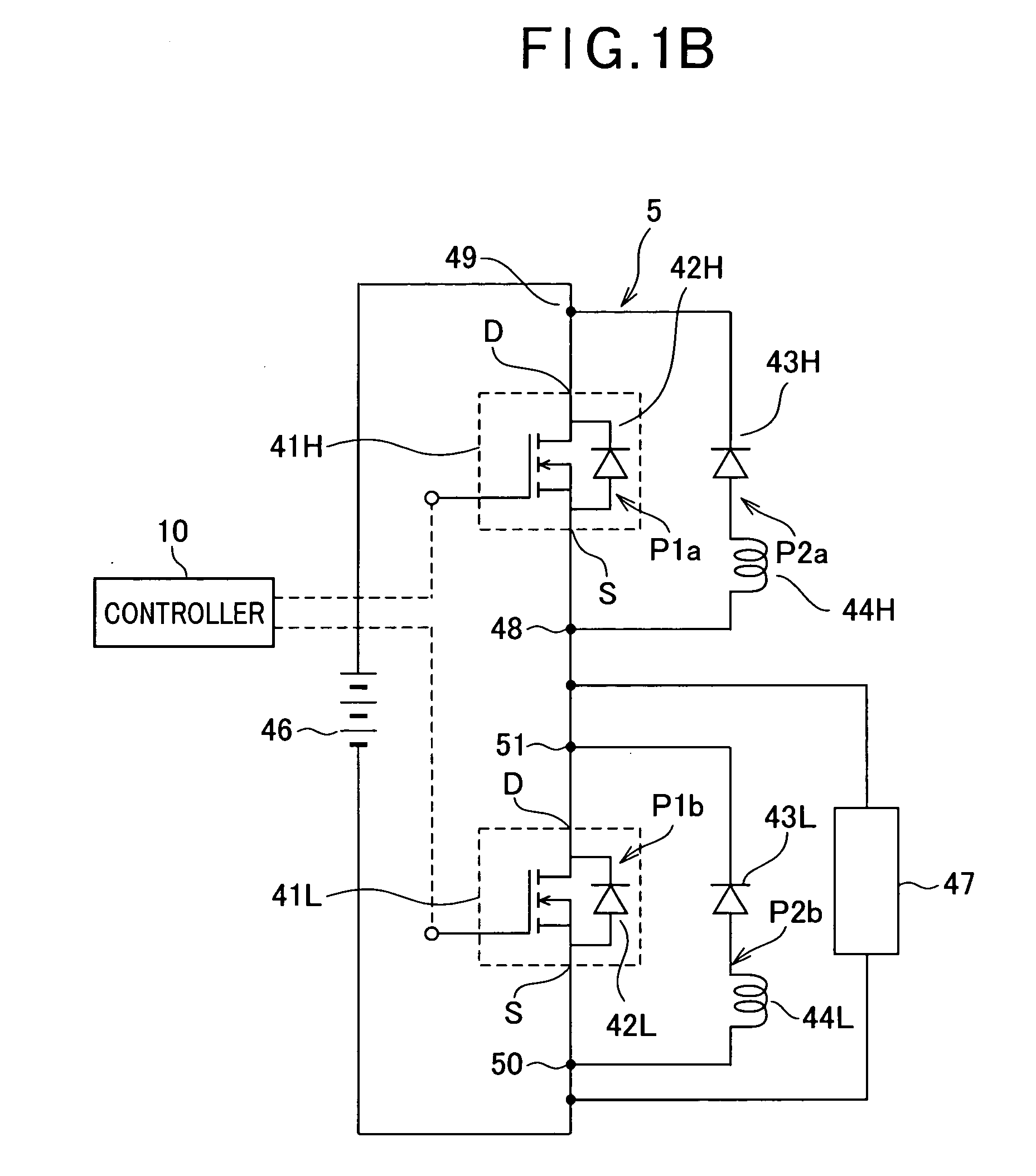
[0042]Referring to FIG. 1A, there is provided a power switching circuit 1 for driving an inductive load 47 according to the embodiment of the present invention.

[0043]The power switching circuit 1 includes a direct current (DC) battery 46 and a half-bridge module 5.

[0044]The half-bridge module 5 includes a pair (bridge arm) of series-connected high-side and low-side MOSFETs 41H and 41L serving as switching elements, intrinsic diodes 4...


PUM


Abstract

In a power switching circuit, a second commutation member has a second commutation path electrically connected in parallel to a first commutation path and a second diode provided in the second commutation path and electrically connected antiparallel to a semiconductor switching element. While the semiconductor switching element is off, the second commutation path allows a second current based on the inductive load to flow therethrough in a forward direction of the second diode within a commutation period. The second diode has a second reverse recovery time shorter than a first reverse recovery time of the first diode. A second inductance of the second commutation path is higher than a first inductance of the first commutation path.

Description

CROSS REFERENCE TO RELATED APPLICATIONS[0001]This application is based on Japanese Patent Application 2008-34524 filed on Feb. 15, 2008. The descriptions of the Patent Application are all incorporated herein by reference.FIELD OF THE INVENTION[0002]The present invention relates to power switching circuits with a switching element for switching on and off the switching element to thereby drive inductive loads. More particularly, the present invention relates to such power switching circuits with a diode connected in antiparallel to the switching element; is diode allows a flywheel current to flow therethrough.BACKGROUND OF THE INVENTION[0003]Semiconductor switching elements are installed in a power converter, such as an inverter, for driving inductive loads, such as motors. In order to bypass a current flowing in a semiconductor switching element when the semiconductor switching element is turned off, a diode is connected in antiparallel to the semiconductor switching element. Specif...

Claims


Application Information

Patent Timeline
IPC IPC(8): G05F1/10
CPCH02M3/1588H03K17/12H03K17/08142Y02B70/1466H01L2224/0603H01L2224/48137H01L2224/48247H01L2224/49111H01L2924/19107H01L2924/13055H01L2924/13091H01L2924/12032H03K17/14Y02B70/10H01L2924/00
Inventor SASAYA, TAKANARIINOUE, TAKESHIKIMURA, TOMONORI
Owner DENSO CORP
Why Eureka
Try Eureka