Method for manufacturing soi substrate

Inactive Publication Date: 2010-04-01
SEMICON ENERGY LAB CO LTD
View PDF41 Cites 0 Cited by
  • Summary
  • Abstract
  • Description
  • Claims
  • Application Information

AI Technical Summary

Benefits of technology

[0010]As disclosed in Reference 2, a single crystal semiconductor layer is irradiated with laser light, whereby the single crystal semiconductor layer is melted and the crystallinity thereof can be improved even in the case of using a glass substrate having low heat resistance or the like.
[0014]In view of the above problems, it is an object of an embodiment of the disclosed invention to provide an SOI substrate having sufficient characteristics in the case of performing laser light irradiation. It is another object to reduce variation in characteristics of an SOI substrate resulting from laser light irradiation conditions.
[0018]In the above embodiment, a glass substrate can be used as the base substrate. The heat treatment may be performed at a temperature higher than or equal to 680° C., preferably, higher than or equal to 700° C., and lower than a strain point of the base substrate. By the laser light irradiation, surface planarity of the semiconductor layer can be improved and defects in the semiconductor layer can be reduced.
[0023]In an embodiment of the disclosed invention, a semiconductor layer in which crystal defects have been sufficiently reduced in advance is irradiated with laser light; thus, an SOI substrate having sufficient characteristics can be obtained also in the case of partial melting by laser light irradiation. In addition, even if irradiation energy density of laser light is lowered, a semiconductor layer having equivalent characteristics can be obtained; thus, it is possible to reduce variation in characteristics of an SOI substrate resulting from variation in energy density of laser light.

Problems solved by technology

In addition, the effect of heat during partial melting leads to crystal defect concentration in the vicinity of a boundary between a melted region and a non-melted region.
Such defects remaining in a non-melted region or in the vicinity of a boundary hinder the improvement in characteristics of finished semiconductor devices and thus cause problems.
However, there is temporal variation in energy density of laser light and thus it is difficult to perform laser light irradiation under constant conditions.
Therefore, variation in energy density of laser light causes variation in characteristics of an SOI substrate, and this leads to a problem of variation in characteristics of a finished semiconductor device.

Method used


Image

  • Method for manufacturing soi substrate
  • Method for manufacturing soi substrate
  • Method for manufacturing soi substrate

Examples


embodiment 1

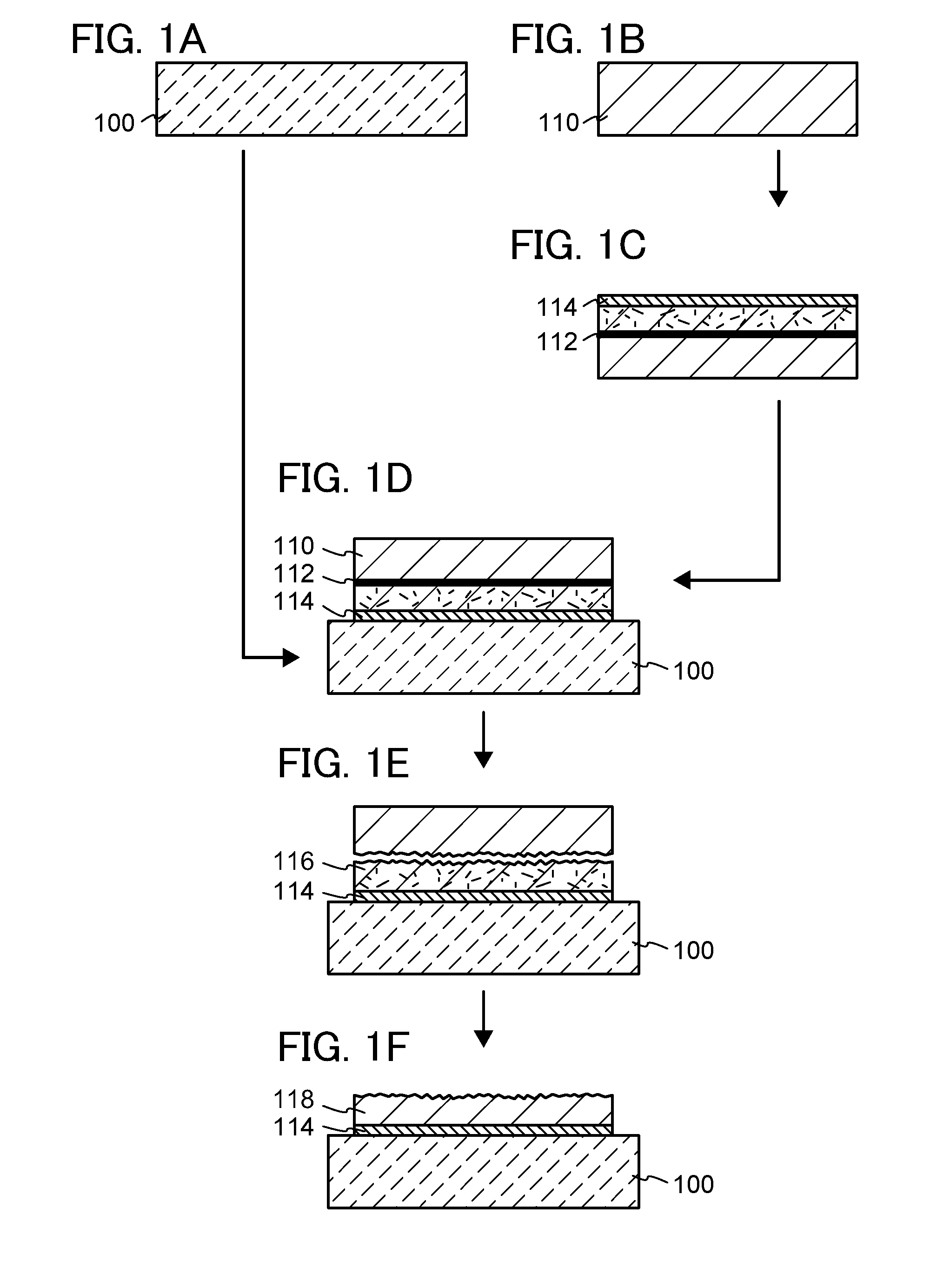
[0035]In this embodiment, an example of a method for manufacturing a semiconductor substrate (an SOI substrate) will be described with reference to drawings. Specifically, the case of manufacturing a semiconductor substrate in which a single crystal semiconductor layer is provided over a base substrate will be described.

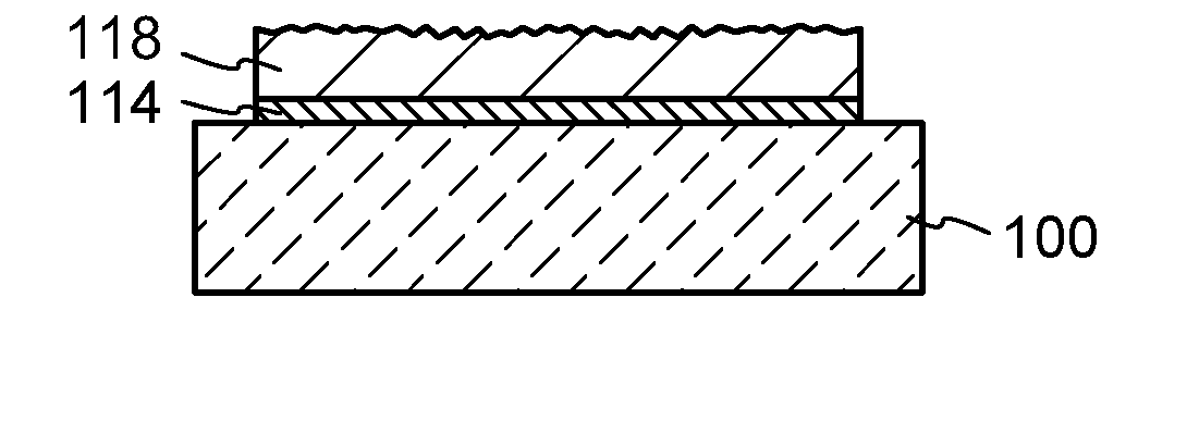
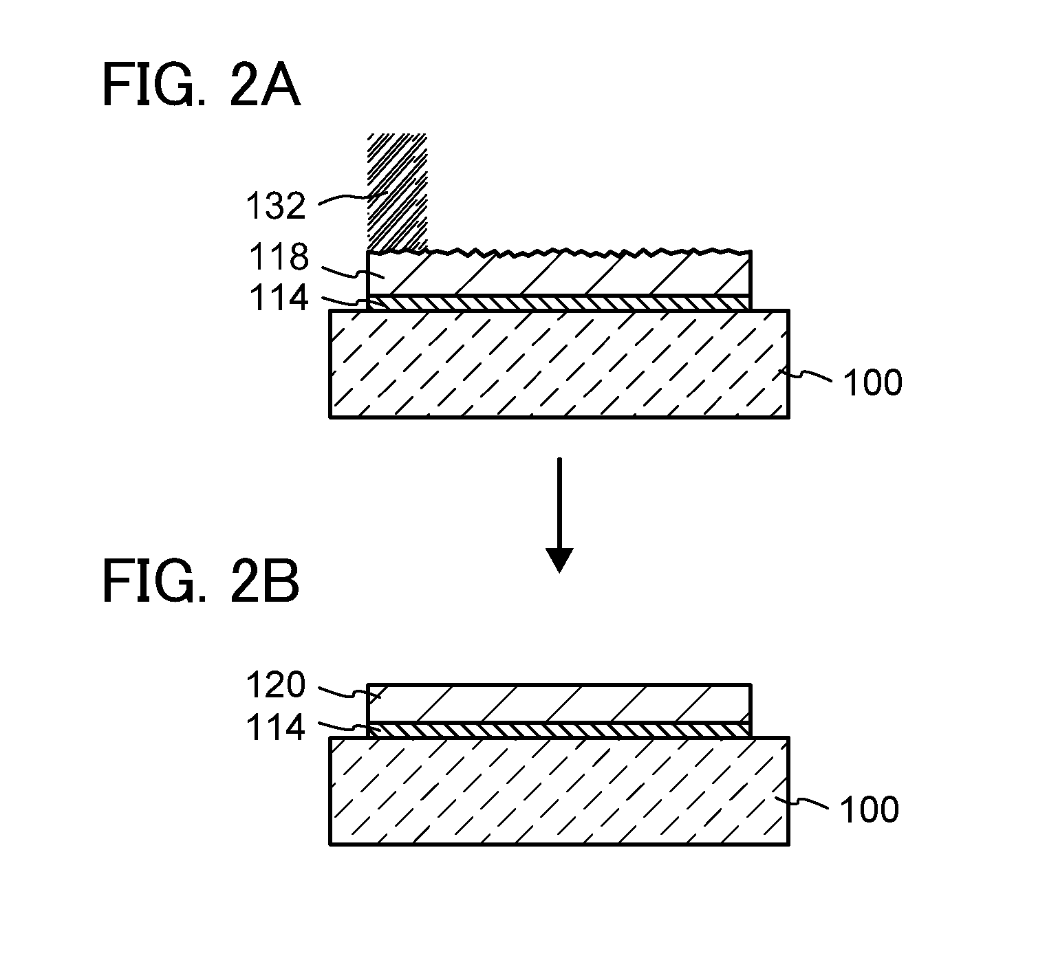
[0036]First, a base substrate 100 and a single crystal semiconductor substrate 110 are prepared (see FIGS. 1A and 1B).

[0037]As the base substrate 100, a substrate made from an insulator can be used. Specific examples thereof include: a variety of glass substrates used in the electronic industries, such as substrates formed with aluminosilicate glass, aluminoborosilicate glass, and barium borosilicate glass; a quartz substrate; a ceramic substrate; and a sapphire substrate. Note that when the above-mentioned glass substrate contains a large amount of boric acid (B2O3), the heat resistance of glass is improved; when it contains a larger amount of barium oxide (BaO) tha...

embodiment 2

[0073]In this embodiment, anther example of a method for manufacturing a semiconductor substrate (an SOI substrate) will be described with reference to drawings.

[0074]First, a base substrate 100 is prepared (see FIG. 3A). The details of the base substrate 100, for which Embodiment 1 can be referred to, are omitted here.

[0075]Next, a nitrogen-containing layer 102 (an insulating film containing nitrogen, such as a silicon nitride (SiNx) film or a silicon nitride oxide (SiNxOy (x>y)) film) is formed over a surface of the base substrate 100 (see FIG. 3B).

[0076]The nitrogen-containing layer 102 formed in this embodiment functions as a layer for bonding a single crystal semiconductor layer (as a bonding layer) in a later step. The nitrogen-containing layer 102 also functions as a barrier layer for preventing an impurity contained in the base substrate, such as sodium (Na), from diffusing into a single crystal semiconductor layer.

[0077]As mentioned above, the nitrogen-containing layer 102 ...

embodiment 3

[0105]In this embodiment, a method for manufacturing a semiconductor device using the above-described semiconductor substrate will be described with reference to FIGS. 5A to 5D, FIGS. 6A to 6D, and FIGS. 7A and 7B. Here, a method for manufacturing a semiconductor device including a plurality of transistors as an example of the semiconductor device is described. Note that various semiconductor devices can be formed with the use of a combination of transistors described below.

[0106]FIG. 5A is a cross-sectional view of a semiconductor substrate which is manufactured in accordance with Embodiment 1.

[0107]In order to control threshold voltages of TFTs, a p-type impurity element such as boron, aluminum, or gallium or an n-type impurity element such as phosphorus or arsenic may be added to a semiconductor layer 500 (corresponding to the single crystal semiconductor layer 120 in Embodiment 1). A region to which the impurity element is added and the kind of impurity element to be added can b...


PUM


Abstract

A single crystal semiconductor substrate is irradiated with accelerated ions to form an embrittled region in the single crystal semiconductor substrate. The single crystal semiconductor substrate and a base substrate are bonded to each other with an insulating layer interposed therebetween. The single crystal semiconductor substrate is separated at the embrittled region to form a semiconductor layer over the base substrate. Heat treatment is performed to reduce defects in the semiconductor layer. The semiconductor layer is then irradiated with laser light.

Description

BACKGROUND OF THE INVENTION[0001]1. Field of the Invention[0002]The invention disclosed herein relates to a method for manufacturing a substrate in which a semiconductor layer is provided over an insulating layer, and particularly relates to a method for manufacturing a silicon-on-insulator (SOI) substrate. The invention also relates to a method for manufacturing a semiconductor device using the substrate.[0003]2. Description of the Related Art[0004]In recent years, integrated circuits formed using, instead of a bulk silicon wafer, a silicon-on-insulator (SOI) substrate where a thin single crystal semiconductor layer is present over an insulating surface have been researched. Because parasitic capacitance generated by a drain of a transistor and a substrate can be reduced by use of an SOI substrate, SOI substrates are attracting attention as substrates which improve performance of semiconductor integrated circuits.[0005]One of known methods for manufacturing SOI substrates is a Smar...

Claims


Application Information

Patent Timeline
IPC IPC(8): H01L21/762
CPCH01L21/76254H01L27/1214H01L27/1266H01L29/66772H01L27/1222H01L21/20
Inventor ISOBE, ATSUOMOMO, JUNPEIOKUNO, NAOKI
Owner SEMICON ENERGY LAB CO LTD
Why Eureka
Try Eureka