

Semiconductor memory device and manufacturing method thereof
- Summary
- Abstract
- Description
- Claims
- Application Information
AI Technical Summary
Benefits of technology
Problems solved by technology
Method used
Image

Examples
first embodiment
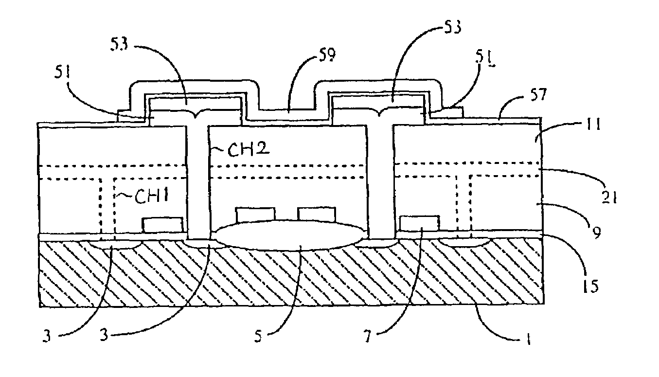
[0061]The first embodiment is described relative to the capacitor of the DRAM. The present invention can also be applied for the structure of the gate electrodes of transistors.
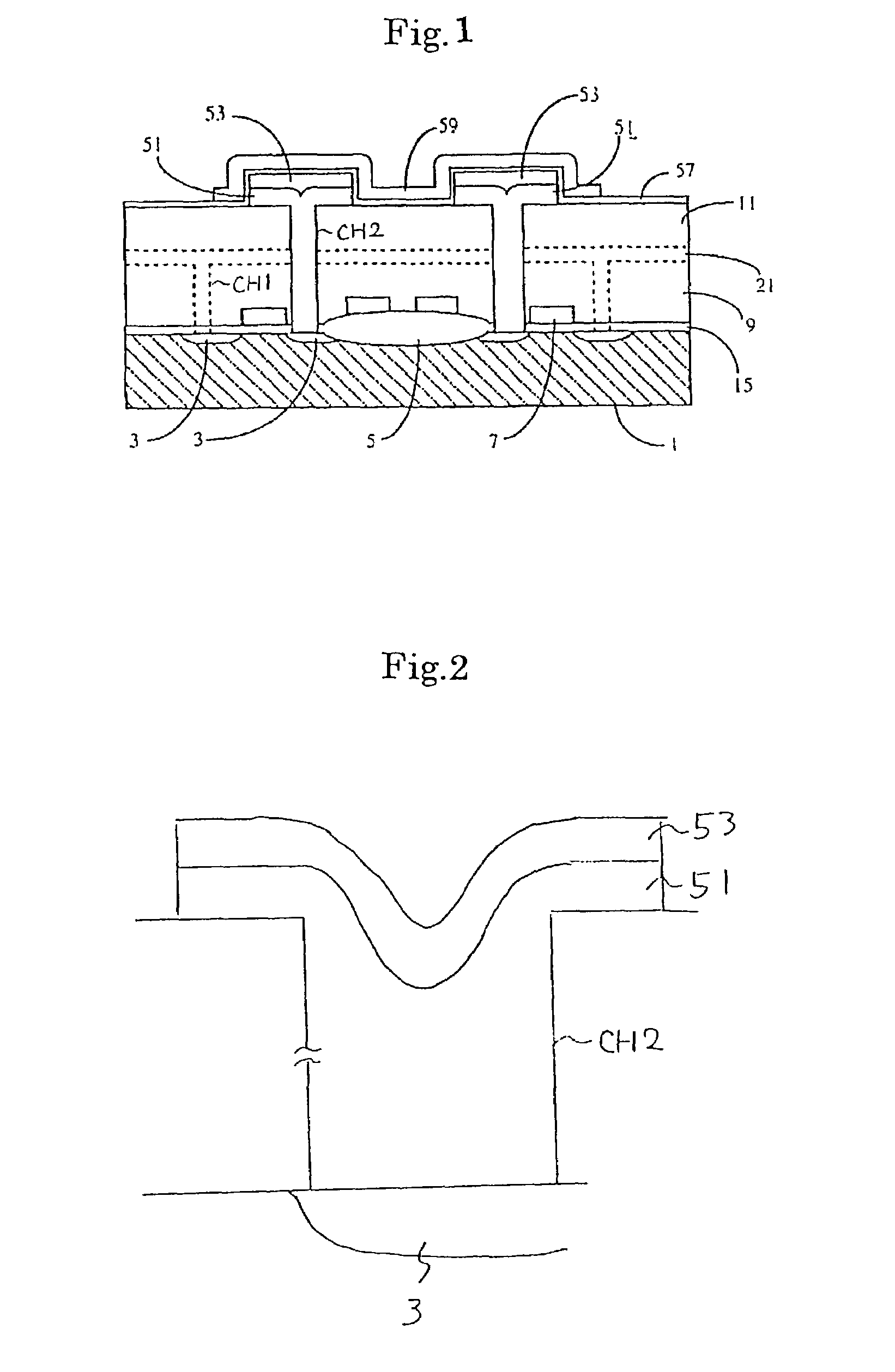
[0062]FIG. 4 is a cross-sectional view describing a memory cell of the DRAM according to a second preferred embodiment. In this embodiment, elements which correspond to the elements of the first preferred embodiment are marked with the same symbols to facilitate understanding.
[0063]In the second preferred embodiment, the surface of the second silicon layer 153 is roughened. That is, the second silicon layer 153 of the storage electrode has a rugged surface 163. Also, the nitride layer 57 formed on the rugged surface 163 has a configuration which according to the rugged surface 163.
[0064]According to this embodiment, as an effective surface area can be increased, the capacitance of the capacitor is increased, compared with the first preferred embodiment. Therefore, a sufficient capacitance which can restrain a...
second embodiment
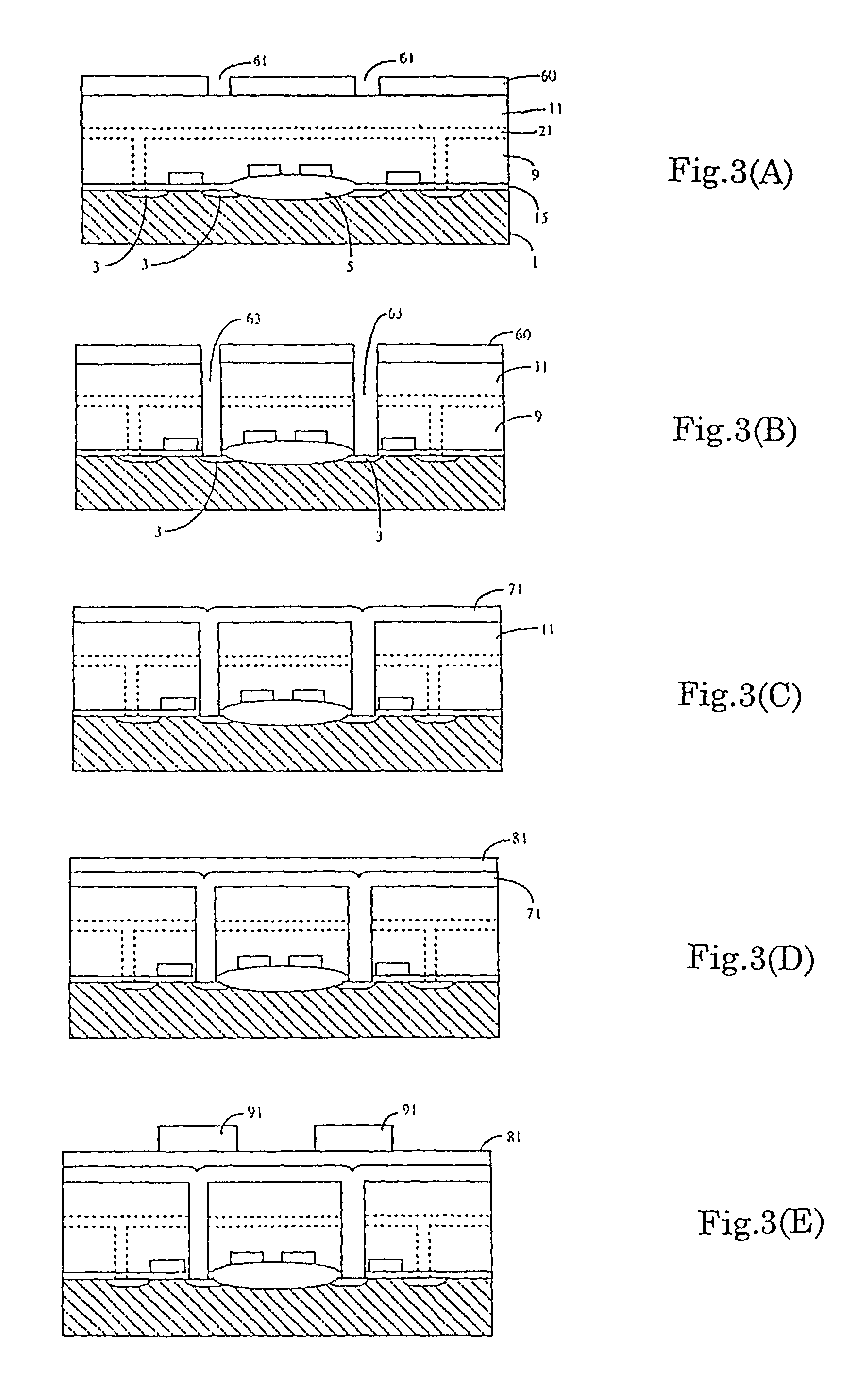
[0065]A method of manufacturing the second embodiment will be shown hereinafter referring to FIG. 5. The explanation below will be focused in the forming of the rugged surface. Before the step of FIG. 5(A), steps similar to those of FIG. 3(A)–FIG. 3(D) are carried out.
[0066]After forming the second silicon layer 81 which is introduced the impurity (phosphorous) on the first silicon layer 71, a rugged polycrystalline silicon layer 160 is formed on the second silicon layer 81. The thickness of the rugged polycrystalline silicon 160 is 500–1000 Å. The rugged polycrystalline silicon layer 160 can be formed in an atmosphere which is introduced with silane SiH4 at a temperature of 560–580° C. Then an anneal treatment is carried out, and the rugged polycrystalline silicon layer 160 becomes conductive. Also, after forming the storage electrode by patterning, the patterned surface of the polycrystalline silicon layer 81 can be roughened.
[0067]A resist layer is formed on the rugged polycrysta...
third embodiment
[0076]A method of manufacturing the third embodiment will be shown hereinafter referring to FIG. 7. The explanation below will be focused on forming the side wall 201. Before the step of FIG. 7(A), steps which corresponds to the steps of FIG. 3(A)–FIG. 3(B) are carried out.
[0077]After the etching step using a resist layer 211 (corresponds to the resist layer 60) as a mask shown in FIG. 3(B), a protection layer 213 is formed in the contact hole and on the resist layer 211. The protection layer 213 is formed using a CVD method and the thickness is 1000–3000 Å, as shown in FIG. 7(A).
[0078]Then, the protection layer 213 is etched by anisotropic etching and the side wall 201 remains on the side of the contact hole, shown in FIG. 7(B). Then the resist layer 211 is removed. After this step, the description of the first embodiment can be referenced.
[0079]The resist layer 211 can be removed before forming the protection layer 213. If the material of the side wall 201 is the same as the secon...
PUM
 Abstract
Description
Claims
Application Information