Semiconductor device and method of manufacturing the same

Active Publication Date: 2010-02-25
MICRON TECH INC
View PDF2 Cites 5 Cited by
  • Summary
  • Abstract
  • Description
  • Claims
  • Application Information

AI Technical Summary

Benefits of technology

[0013]Accordingly, a thickness and a height of the silicon thin film forming the channel can be controlled with high precision and reproducibility. Therefore, a threshold voltage of the semiconductor device can be controlled, and fluctuations in characteristics of the semiconductor device can be reduced.

Problems solved by technology

Accordingly, a great amount of substrate current flows which cannot be controlled by a gate.
In other words, short-channel effects have been becoming more problematic.
However, an increase in junction leakage current or gate voltage has been problematic though the short channel effect can be prevented.
However, in the method of manufacturing the three-dimensional SOI channel disclosed in the above related art, it is difficult to form the fin-shaped SOI channel with high precision and reproducibility since the fin-shaped SOI chapel is formed by processing the gate trench using a mask used for the formation of the STI.
For this reason, it is difficult to control the threshold voltage of the transistor.

Method used


Image

  • Semiconductor device and method of manufacturing the same
  • Semiconductor device and method of manufacturing the same
  • Semiconductor device and method of manufacturing the same

Examples


first embodiment

[0025]A first embodiment of the present invention explains the case where the present invention is applied to a trench gate FET (Field Effect Transistor) in a DRAM memory cell array.

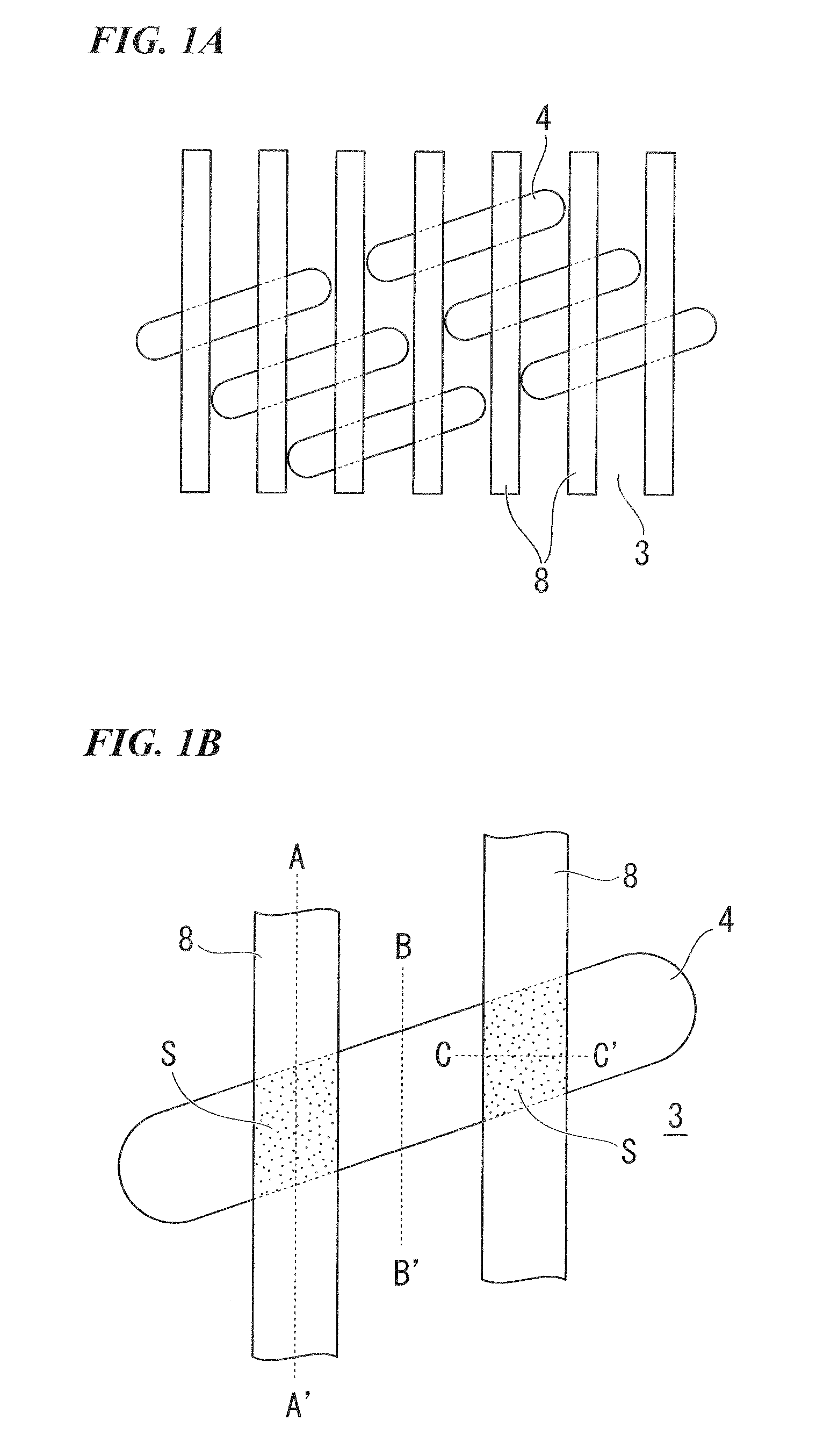
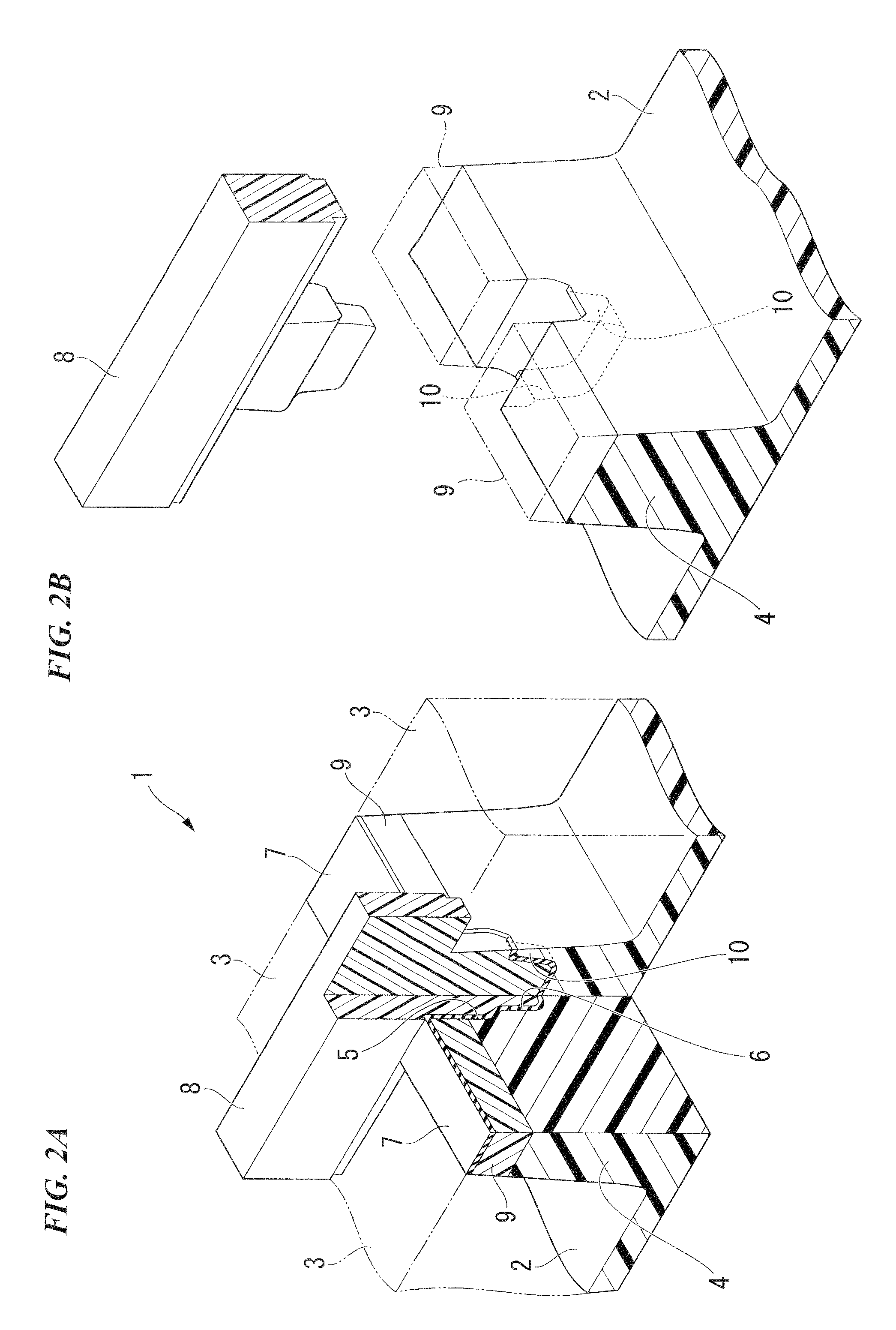
[0026]In a DRAM memory cell as shown in FIG. 1A, active regions 4 are defined by an STI region 3. Gate electrodes 8 which will be word lines are formed across the active regions 4. As shown in FIG. 1B a cross region where the active region 4 crosses the gate electrode 8 is a trench gate formation region S. As shown in FIG. 2A, a trench gate FET 1 is formed in the trench gate formation region S.

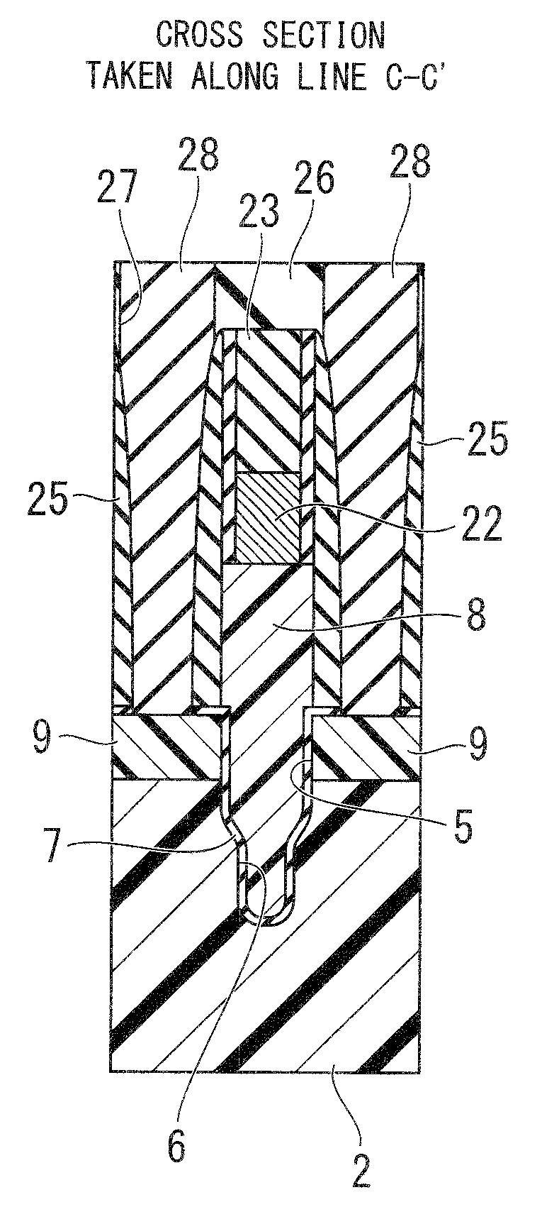
[0027]The trench gate FET 1 includes: a semiconductor substrate 2 having a surface layer including silicon; an STI region 3 made of an insulating film embedded in the semiconductor substrate 2; an active region 4 defined by the STI region 3; a first gate trench 5 formed in the active region 4; a second gate trench 6 directly below the first gate trench 5; a gate electrode 8 embedded into the first and second gate t...

second embodiment

[0078]Hereinafter, a method of manufacturing a semiconductor device according to a second embodiment of the present invention is explained with reference to FIGS. 22 to 24. The method according to the second embodiment is different from the method of manufacturing the trench gate FET1 according to the first embodiment. Like reference numerals denote like elements between the first and second embodiments, and explanations thereof are omitted.

[0079]In the method of manufacturing the trench gate FET1 according to the second embodiment, a silicon oxide film is formed by CVD in place of the silicon oxide film 19 which is formed by thermal oxidation and shown in FIG. 12. The processes up to the process of forming the first gate trench 5 shown in FIG. 11 in the first embodiment are the same in the second embodiment. Therefore, explanations thereof are omitted.

[0080]After the first gate trench 5 is formed, a silicon oxide film 29 having a thickness of 20 nm is deposited over the entire surf...


PUM


Abstract

A method of manufacturing a semiconductor device includes the following processes. A first gate trench is formed if a semiconductor substrate region. Then a first insulating film is formed to cover bottom and side surfaces of the first gate trench. Then, the first insulating film is removed to cover the bottom surface. Then, the semiconductor substrate region exposed to the first gate trench is etched by the first insulating film covering the side surfaces as a mask, to form, in the semiconductor substrate region, a second gate trench directly below the first gate trench. The second gate trench is defined by an unetched film portion of the semiconductor substrate region. The unetched film portion extends toward one of the side surfaces of the first gate trench.

Description

BACKGROUND OF THE INVENTION[0001]1. Field of the Invention[0002]The present invention relates to a semiconductor device and a method of manufacturing the same.[0003]Priority is claimed on Japanese Patent Application No. 2008-210556, filed Aug. 19, 2008, the content of which is incorporated herein by reference.[0004]2. Description of the Related Art[0005]Recently, gate lengths of MOS (Metal Oxide Semiconductor) transistors are shorter and shorter as semiconductor devices, such as a DRAM (Dynamic Random Access Memory), are further miniaturized. Accordingly, a great amount of substrate current flows which cannot be controlled by a gate. In other words, short-channel effects have been becoming more problematic.[0006]In an MOS transistor used for a cell array transistor DRAM, a concentration of an impurity included in a channel region is increased to prevent such a short channel effect. However, an electric field around an S / D junction increases as a concentration of an impurity included...

Claims


Application Information

Patent Timeline
IPC IPC(8): H01L29/78H01L21/336
CPCH01L21/823437H01L27/10876H01L29/785H01L29/66795H01L27/10879H10B12/056H10B12/053
Inventor SUGIOKA, SHIGERU
Owner MICRON TECH INC
Why Eureka
Try Eureka