

Method of manufacturing soi substrate
- Summary
- Abstract
- Description
- Claims
- Application Information
AI Technical Summary
Benefits of technology
Problems solved by technology
Method used
Image

Examples
embodiment 1
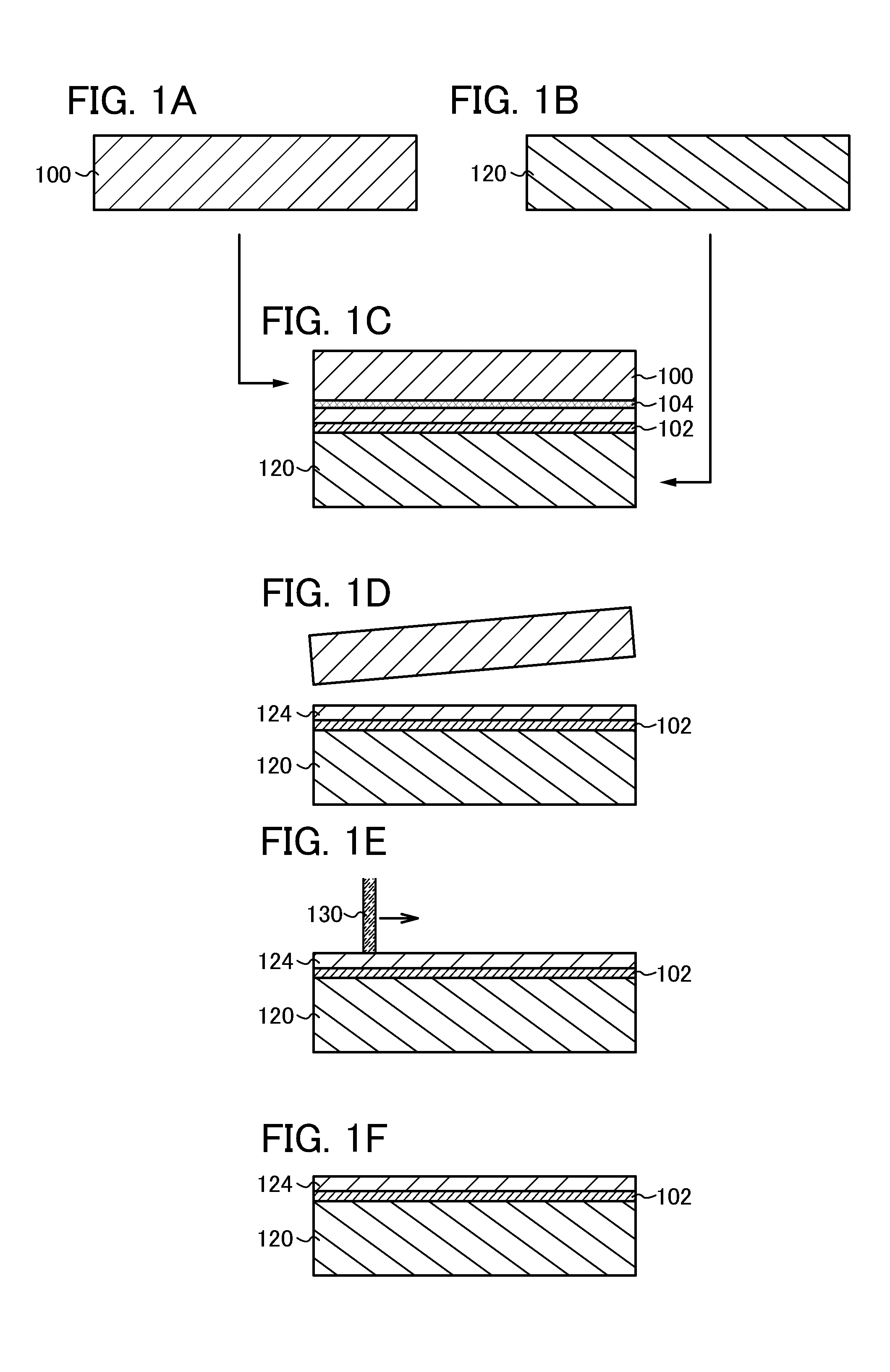
[0035]This embodiment will describe an example of a method of manufacturing a semiconductor device with reference to drawings. In particular, the case of manufacturing a semiconductor device using a single crystal semiconductor layer provided over a base substrate is described.
[0036]First, a single crystal semiconductor substrate 100 and a base substrate 120 are prepared (see FIGS. 1A and 1B).
[0037]As the single crystal semiconductor substrate 100, a single crystal semiconductor substrate formed using an element of Group 14, such as a single crystal silicon substrate, a single crystal germanium substrate, or a single crystal silicon germanium substrate, can be used. Alternatively, a compound semiconductor substrate formed using such as gallium arsenide or indium phosphide, can be used. The size of a commercial silicon substrate is typically a circular substrate which is 5 inches (125 mm) in diameter, 6 inches (150 mm) in diameter, 8 inches (200 mm) in diameter, 12 inches (300 mm) in...
embodiment 2
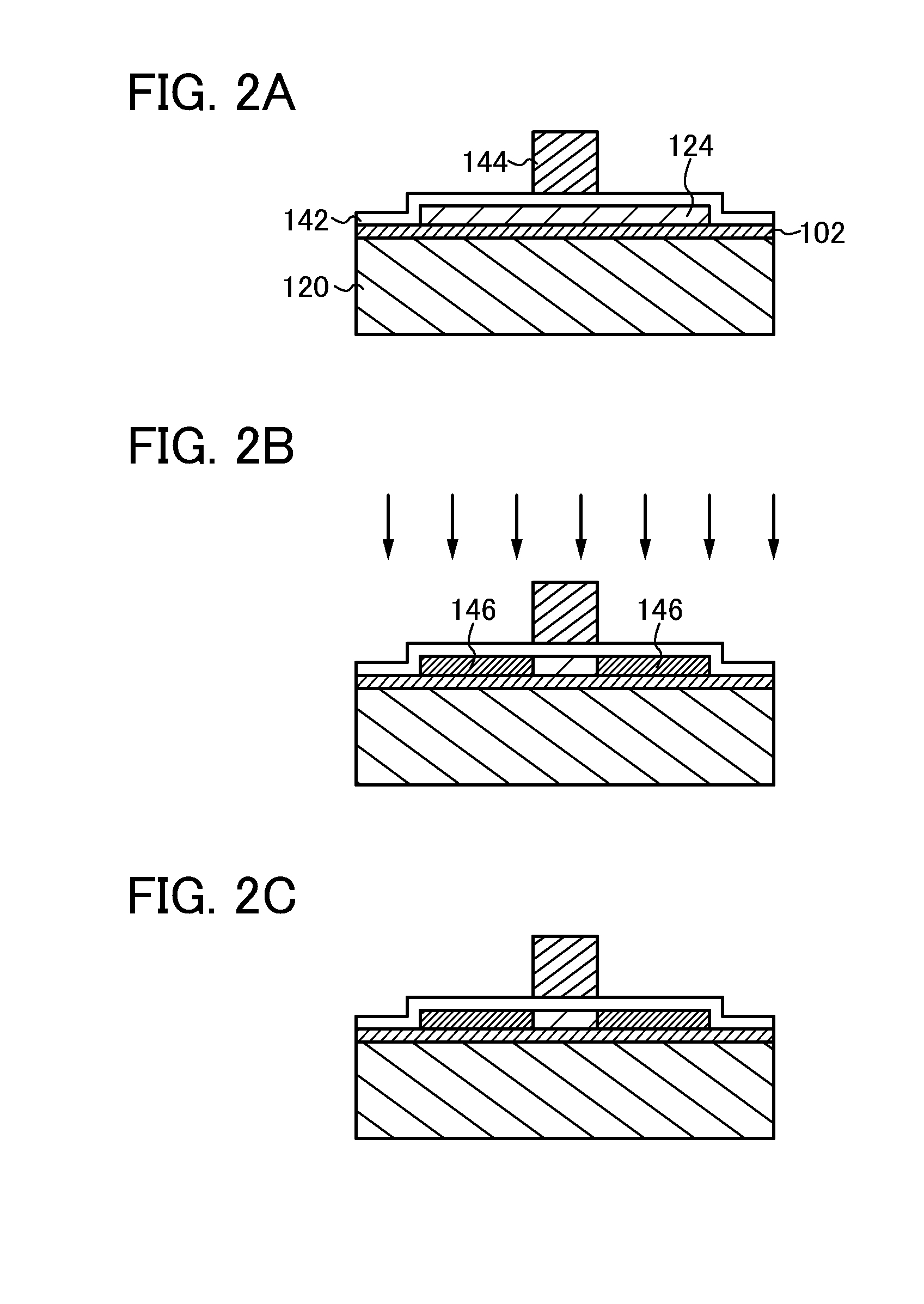
[0071]This embodiment will describe an example of attaching the single crystal semiconductor substrate 100 to the base substrate 120 with reference to drawings.
[0072]First, the single crystal semiconductor substrate 100 is prepared (see FIG. 3(A-1)). It is preferable that the surface of the single crystal semiconductor substrate 100 be cleaned using a sulfuric acid / hydrogen peroxide mixture (SPM), an ammonium hydroxide / hydrogen peroxide mixture (APM), a hydrochloric acid / hydrogen peroxide mixture (HPM), dilute hydrogen fluoride (DHF), or the like as appropriate in advance in terms of removing contaminations. Alternatively, dilute hydrogen fluoride and ozone water may be discharged alternately to clean the surface of the single crystal semiconductor substrate 100.
[0073]Next, an oxide film 132 is formed on the surface of the single crystal semiconductor substrate 100 (see FIG. 3(A-2)).
[0074]As the oxide film 132, for example, a single layer of a silicon oxide film, a silicon oxynitrid...
embodiment 3
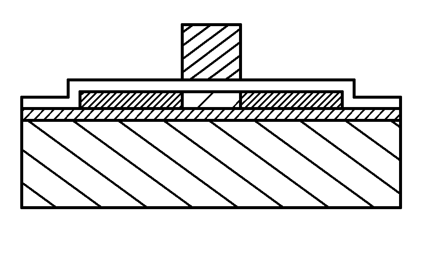
[0123]This embodiment will describe a method of manufacturing a semiconductor device having a transistor, using the SOI substrate manufactured according to the above embodiments.
[0124]First, a method for manufacturing an n-channel thin film transistor and a p-channel thin film transistor will be described with reference to FIGS. 4A to 4D and FIGS. 5A to 5C. Various kinds of semiconductor devices can be formed by combining a plurality of thin film transistors (TFTs).
[0125]This embodiment will describe the case where the SOI substrate manufactured using the process of FIGS. 3(A-1) to 3(A-3), 3(B-1) and 3(B-2), 3C, and 3D is used as an SOI substrate. Needless to say, an SOI substrate which is manufactured using any other method described in the above embodiments can be used.
[0126]FIG. 4A is a cross-sectional view of the SOI substrate which is manufactured using the method described in FIGS. 3(A-1) to 3(A-3), 3(B-1) and 3(B-2), 3C, and 3D.
[0127]First, the single crystal semiconductor la...
PUM
 Abstract
Description
Claims
Application Information