
Semiconductor integrated circuit

a technology of integrated circuits and semiconductors, applied in the direction of logic circuits characterised by logic functions, pulse techniques, transistors, etc., can solve the problems of difficult to ensure the stability of a specified circuit composing the semiconductor integrated circuit, the power source voltage and the threshold voltage of a mos element cannot follow the ideal scaling rule for the process, and the problem of reducing the area overhead, reducing the area, and reducing the overhead area

Inactive Publication Date: 2009-08-20
SOCIONEXT INC
View PDF9 Cites 4 Cited by
  • Summary
  • Abstract
  • Description
  • Claims
  • Application Information

AI Technical Summary

Benefits of technology

[0008]The present invention has been achieved to solve the problem of the area overhead in the layout of the semiconductor integrated circuit mentioned above and it is therefore an object of the present invention to provide a semiconductor integrated circuit occupying a smaller area and free from the degradation of the circuit characteristics.
[0010]The arrangement allows a reduction in area overhead because the substrate of the second polarity that has been conventionally inserted between the two substrates each of the first polarity is no more necessary. As a result, it becomes possible to achieve a further area reduction and implement a high-performance semiconductor integrated circuit occupying a smaller area.
[0011]The semiconductor integrated circuit according to the present invention is extremely useful in implementing a high-performance semiconductor chip which is smaller in area and lower in power consumption, ensures a long battery lifetime with a future chip set supplied with power from a battery or the like, and can provide the chip set with a lower-cost and higher-performance semiconductor chip owing to the area reduction.

Problems solved by technology

However, in the recent 0.13-μm to 90-nm generation, a situation has been encountered in which the power source voltage and the threshold voltage of a MOS element cannot follow the ideal scaling rule for the process.
One reason for this is that, in the current situation, it is difficult to ensure the stability of a specified circuit composing the semiconductor integrated circuit.
When the dynamic circuit is physically placed, an overhead of the area occupied by the isolation region (region 100 enclosed in each of the broken rectangles in FIG. 8) has presented a problem.

Method used


Image

  • Semiconductor integrated circuit
  • Semiconductor integrated circuit
  • Semiconductor integrated circuit

Examples


embodiment 1

[0021]The first embodiment of the present invention shows an example of the placement of a semiconductor integrated circuit for supplying optimal substrate potentials to MOS transistors in a dynamic circuit.

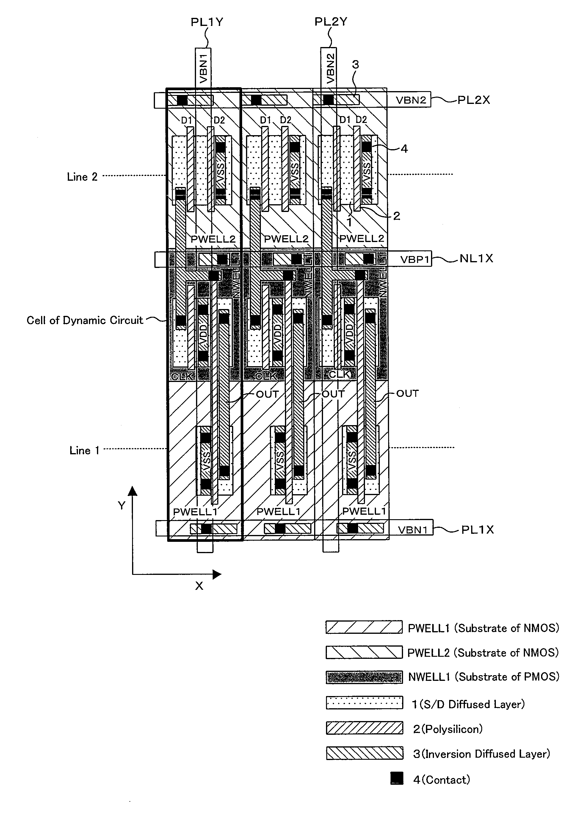
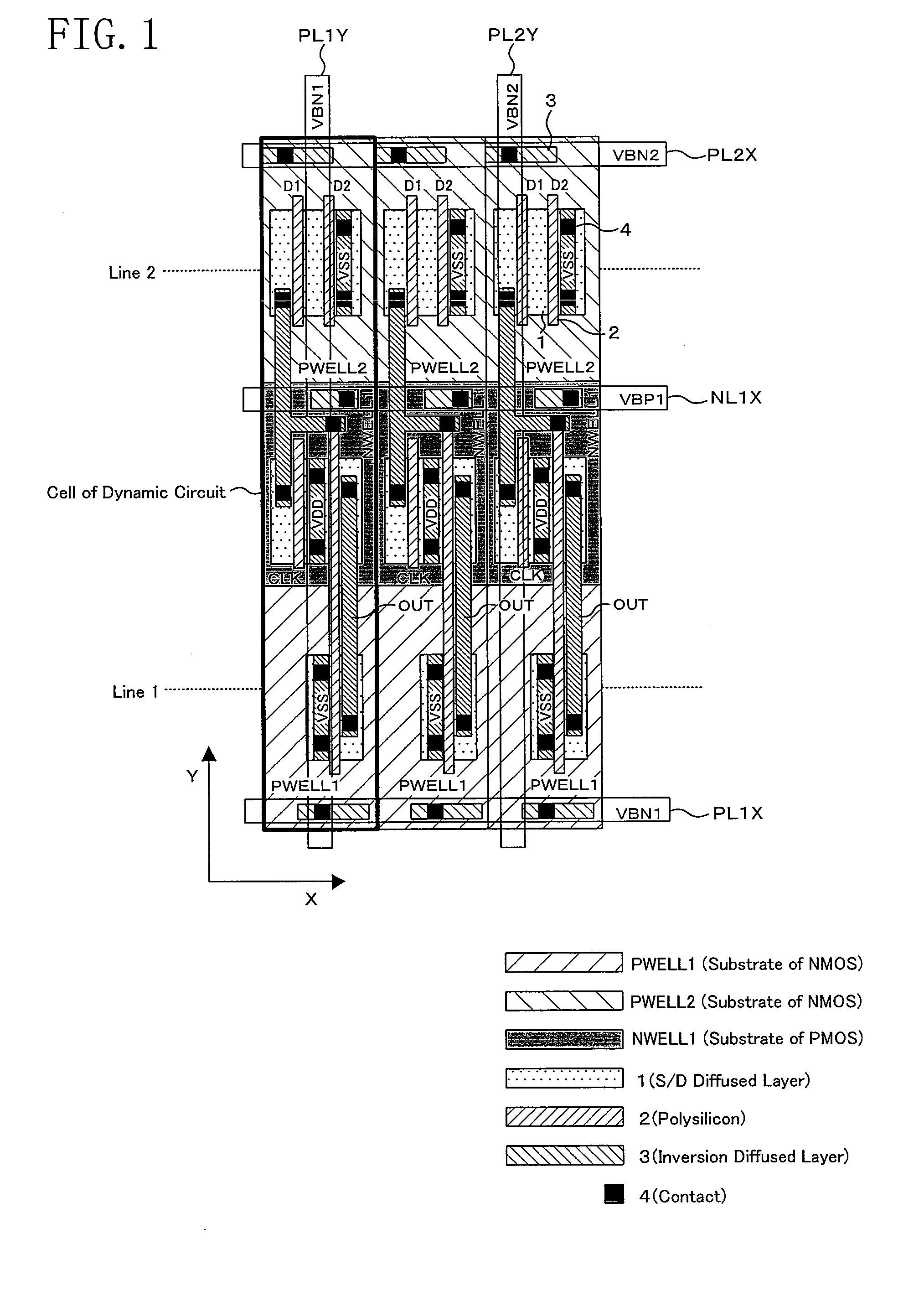
[0022]FIG. 1 is a layout diagram in which the elements composing the dynamic circuit of FIG. 7 are physically arranged.

[0023]In FIG. 1, each of the elements comprises: NMOS substrates PWELL1 and PWELL2; a PMOS substrate NWELL1; polysilicon 2 composing the respective gates of the MOS transistors; S / D diffused layers 1 forming the source / drain of each of the MOS transistors; an inversion diffused layer 3 for supplying a potential to each of the substrates; and contacts 4 providing connection between a first metal layer as the lowermost metal layer and each of the inversion diffused layer 3, the diffused layers 1, and the gates 2. Upper metal layers provided over the first metal layer are normally used for connection between the inputs and outputs of individual circuits, power sourc...

embodiment 2

[0033]The first embodiment has described the case where the dynamic circuits are repeatedly arranged. The second embodiment will describe the case where the dynamic circuit is mounted together with another logic circuit on one chip. FIG. 3 shows a layout structure of the basic structure of the second embodiment. The structure of FIG. 3 is obtained when a 2-input NAND circuit is placed on the right side of the dynamic circuit and a 2-input NOR circuit is placed on the left side thereof. When the number of series-connected NMOS transistors is large, they are disposed on the substrate PWELL2. Conversely, when the number of series-connected NMOS transistors is small, they are disposed on the substrate PWELL1. As the number of series-connected MOS transistors is larger, a drain leakage current is reduced under the DIBL (Drain Induced Barrier Lowering) effect. When the number of series-connected MOS transistors is two, the drain leakage current is about 25% of that when there are no serie...

embodiment 3

[0034]FIG. 4 shows a layout structure of a semiconductor integrated circuit according to the third embodiment of the present invention. FIG. 5 is a cross-sectional view thereof. In the structure of FIG. 4, a normal CMOS circuit exists on a lateral side of the physically placed semiconductor integrated circuit of FIG. 1 such that the semiconductor integrated circuit of FIG. 1 is surrounded by the substrate NWELL2, whereby the substrate NWELL2 is grounded. By thus disposing the substrate NWELL2 between the substrate NWELL1 and a substrate NWELL3, a latch-up can be prevented.

[0035]For example, in the case where the substrate NWELL2 is not provided, when the potential at the point A between the deeper substrate NWELL of a P-substrate and the substrate NWELL3, which should originally be 0 V, has reached, e.g., 1.1 V due to a high resistance as shown in FIG. 6(a), a current Ic1 flows from the substrate NWELL3 to the deeper substrate NWELL. As a result, the voltage of the substrate NWELL1 ...


PUM


Abstract

A semiconductor integrated circuit has a first substrate of a first polarity to which a first substrate potential is given, a second substrate of the first polarity to which a second substrate potential different from the first substrate potential is given, and a third substrate of a second polarity different from the first polarity. The first substrate is insulated from a power source or ground to which a source of a MOSFET formed on the substrate is connected. The third substrate is disposed between the first and second substrates in adjacent relation to the first and second substrates. A circuit element is formed on the third substrate.

Description

CROSS REFERENCE TO RELATED APPLICATIONS[0001]The teachings of Japanese Patent Application JP 2005-224247, filed Aug. 2, 2005, are entirely incorporated herein by reference, inclusive of the specification, drawings, and claims.BACKGROUND OF THE INVENTION[0002]1. Field of the Invention[0003]The present invention relates to a semiconductor integrated circuit comprising at least two independent substrates of the same one polarity and at least one substrate of another different polarity and, more particularly, to a technology for reductions in area and power consumption.[0004]2. Description of the Prior Art[0005]In a semiconductor integrated circuit, the substrate potential of a MOS element (MOS transistor) is used occasionally under control. This is because, by changing the substrate potential of the MOS element, an advantageous feature is provided that the threshold and saturation current characteristic of the MOS element can be varied. As an example of making use of the advantageous f...

Claims


Application Information

Patent Timeline
Patent Type & Authority Applications(United States)
IPC IPC(8): H03K19/096H01L27/088H03K19/0944
CPCH01L27/0928H01L2924/0002H01L2924/00
Inventor SUMITA, MASAYA
Owner SOCIONEXT INC
Learn More