Supercharge Your Innovation With Domain-Expert AI Agents!

Clock recovery circuit

Inactive Publication Date: 2009-08-20
HITACHI LTD
View PDF3 Cites 17 Cited by
  • Summary
  • Abstract
  • Description
  • Claims
  • Application Information

AI Technical Summary

Benefits of technology

[0018]The invention has been made in order to solve the above-mentioned problems, and an object of the invention is to provide a clock recovery circuit capable of simultaneously satisfying three requirements, required for a clock recovery circuit for burst transmission, that is, a short bit synchronization period, a clock wander tracking performance, and a high high-frequency jitter tolerance.
[0021]That is, a clock recovery circuit according to the representative embodiment of the invention includes a first feedback path that is used during general data transmission and averages a phase difference between a recovery clock and an input data signal to adjust a clock phase and a second feedback path that is used only at a burst transmission start time and rapidly changes the phase of the recovery clock. In this way, it is possible to simultaneously satisfy requirements required for a clock recovery circuit for burst transmission, that is, a short bit synchronization period, a clock wander tracking performance, and a high high-frequency jitter tolerance.
[0022]In the clock recovery circuit according to the representative embodiment, the second feedback path that changes the phase of the recovery clock at a high-speed at the burst transmission start time may be slowly reset during a normal operation. In this way, it is not necessary to reset the second feedback path that changes the phase of an internal clock at a high-speed, and it is possible to shorten the time interval between burst transmission operations.
[0023]According to the representative embodiment of the invention, it is possible to provide a clock recovery circuit having a short bit synchronization period, a clock wander tracking performance, and a high jitter tolerance.

Problems solved by technology

The clock recovery circuit disclosed in the above-mentioned paper has a short bit synchronization period and a clock wander tracking performance, but has a low high-frequency jitter tolerance.

Method used


Image

  • Clock recovery circuit
  • Clock recovery circuit
  • Clock recovery circuit

Examples


first embodiment

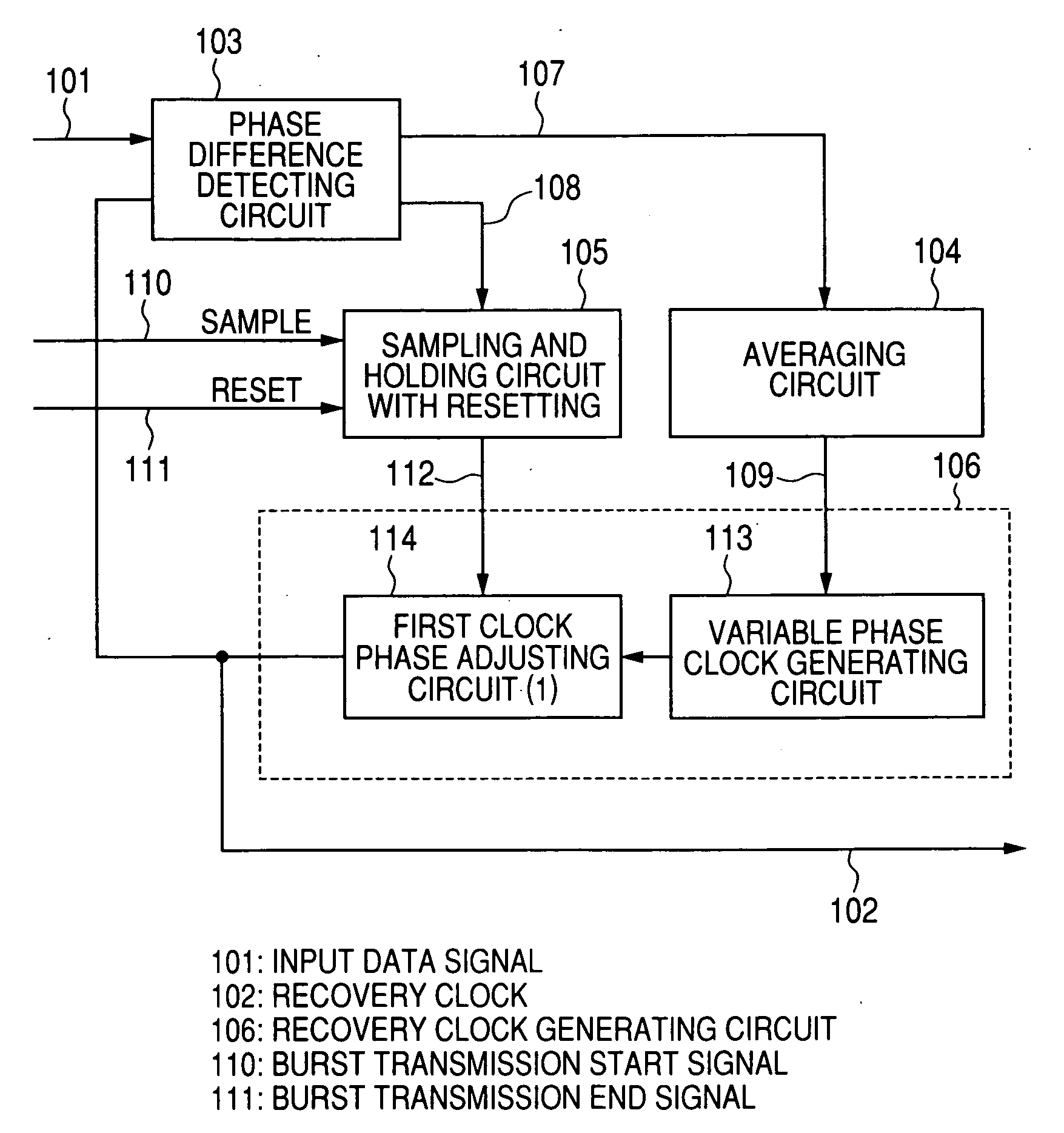
[0036]FIG. 1 is a block diagram illustrating an example of the structure of a clock recovery circuit according to a first embodiment of the invention. The clock recovery circuit according to the first embodiment includes a phase difference detecting circuit 103 (first circuit) that receives an input data signal 101 and outputs a recovery clock 102, an averaging circuit 104 (second circuit), a sampling and holding circuit 105 with resetting (third circuit), and a recovery clock generating circuit 106 (fourth circuit). The recovery clock generating circuit 106 includes a variable phase clock generating circuit 113 (sixth circuit) and a first clock phase adjusting circuit 114 (seventh circuit).

[0037]The clock recovery circuit according to the first embodiment is composed of, for example, a semiconductor integrated circuit, and is formed on one semiconductor chip by a known semiconductor manufacturing technique.

[0038]The phase difference detecting circuit 103 detects a phase difference ...

second embodiment

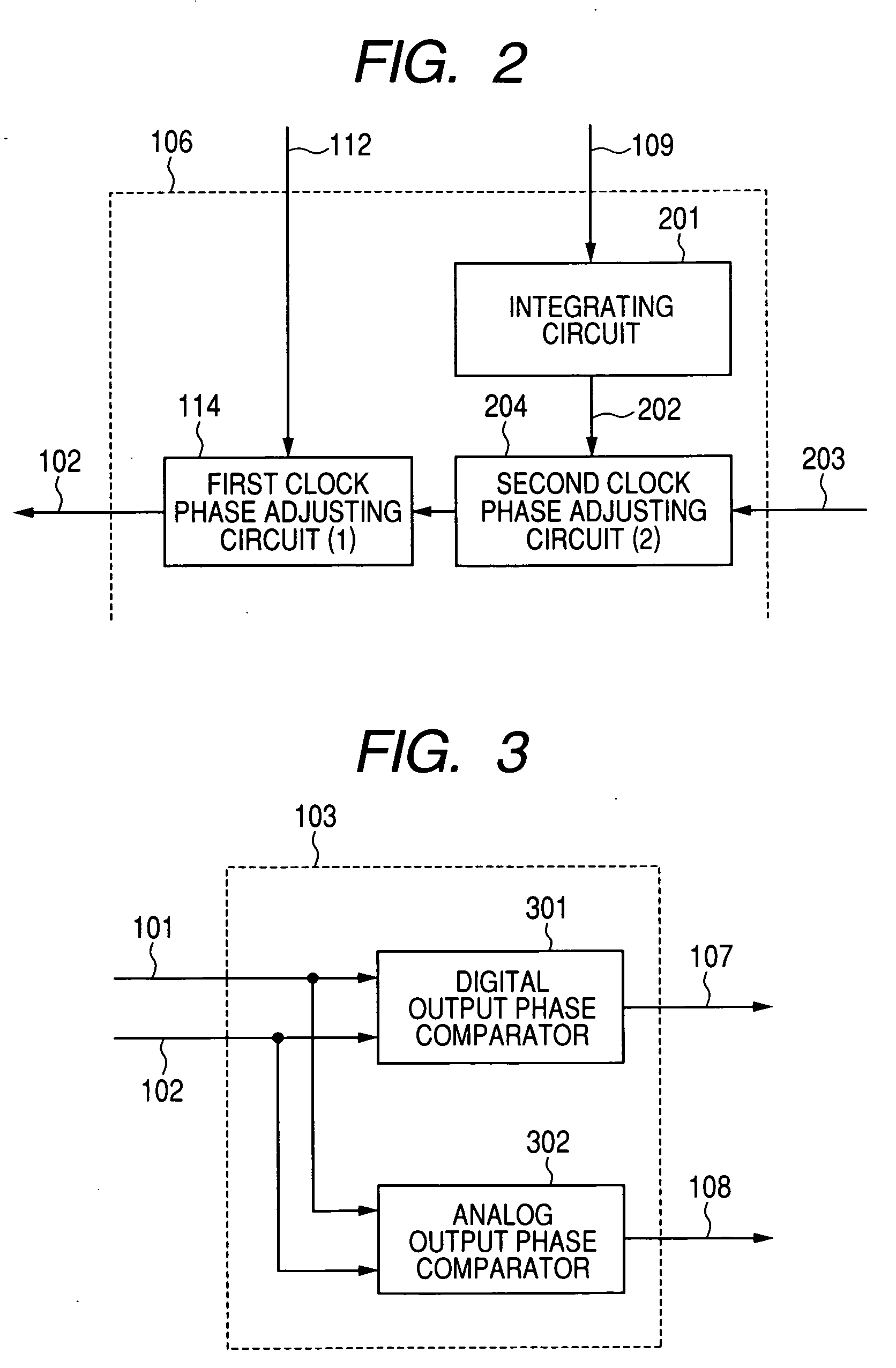
[0056]FIG. 5 is a block diagram illustrating an example of the structure of a clock recovery circuit according to a second embodiment of the invention. The clock recovery circuit according to the second embodiment is similar to that according to the first embodiment except that the sampling and holding circuit 105 with resetting is substituted for a sampling and holding circuit 501 (fifth circuit) with leakage.

[0057]The sampling and holding circuit 501 with leakage samples and holds the high-speed phase difference signal 108 in synchronization with a burst transmission start signal 110 input from the outside at a burst transmission start time, and outputs a high-speed clock phase adjusting signal 112. However, leakage occurs in the holding operation, and the high-speed clock phase adjusting signal 112 is slowly changed to zero, which is an initial value. The change speed of the high-speed clock phase adjusting signal 112 due to the leakage is sufficiently lower than the change speed...


PUM


Abstract

A clock recovery circuit capable of simultaneously satisfying all of a bit synchronization period, a clock wander tracking performance, and a high high-frequency jitter tolerance. The clock recovery circuit includes: a phase difference detecting circuit that detects a phase difference between an input data signal and a recovery clock; an averaging circuit that averages the output of the phase difference detecting circuit; a sampling and holding circuit with resetting that samples and holds the output of the phase difference detecting circuit; and a recovery clock generating circuit that generates a recovery clock having a phase corresponding to the sum of the integral value of the output of the averaging circuit and the output of the sampling and holding circuit with resetting. The sampling and holding circuit with resetting receives a burst transmission start signal and samples and holds the output of the phase difference detecting. In addition, the sampling and holding circuit with resetting receives a burst transmission end signal and resets the held value to an initial value.

Description

CLAIM OF PRIORITY[0001]The present application claims priority from Japanese patent application JP 2008-037088 filed on Feb. 19, 2008, the content of which is hereby incorporated by reference into this application.FIELD OF THE INVENTION[0002]The present invention relates to a clock recovery circuit and more particularly to a technique for recovering a clock signal from a received data signal.BACKGROUND OF THE INVENTION[0003]The inventors have examined the following techniques applicable to, for example, a clock recovery circuit.[0004]FIG. 7 is diagram illustrating a PON (passive optical network) system according to the related art. The PON system is constructed by connecting an OLT (optical line terminal) 701 installed in the central office of a communication service provider and ONUs (optical network units) 702-n (n is a natural number) installed at plural user sites using an optical fiber 703 and a coupler 704 that branches the optical fiber.[0005]Data signals are transmitted as a...

Claims


Application Information

Patent Timeline
IPC IPC(8): H04L7/00
CPCH03L7/081H03L7/0812H04L7/10H04L7/027H04L7/033H03L7/087H04L7/0276
Inventor FUKUDA, KOJIYAMASHITA, HIROKI
Owner HITACHI LTD
Features
  • R&D
  • Intellectual Property
  • Life Sciences
  • Materials
  • Tech Scout
  • Unparalleled Data Quality
  • Higher Quality Content
  • 60% Fewer Hallucinations
Learn More