In-Situ Formed Capping Layer in MTJ Devices

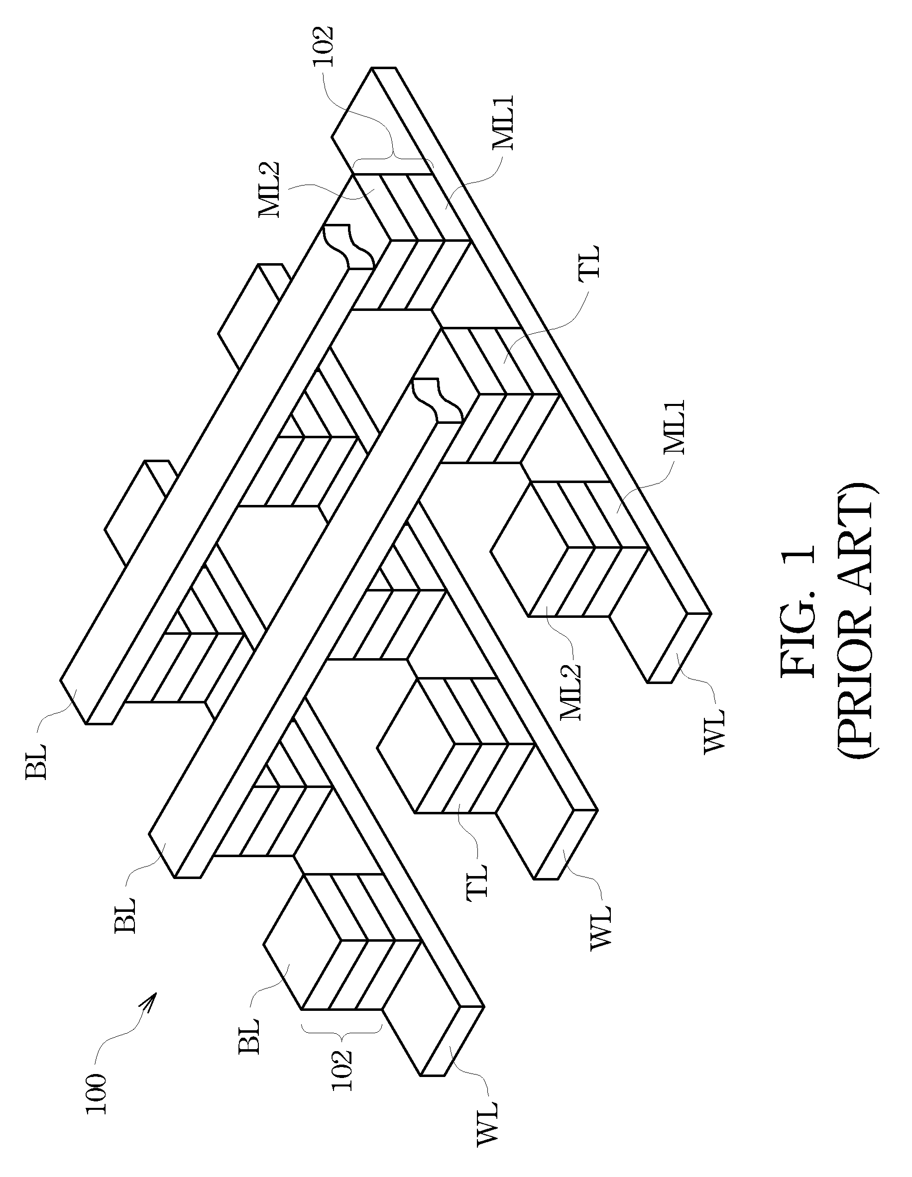
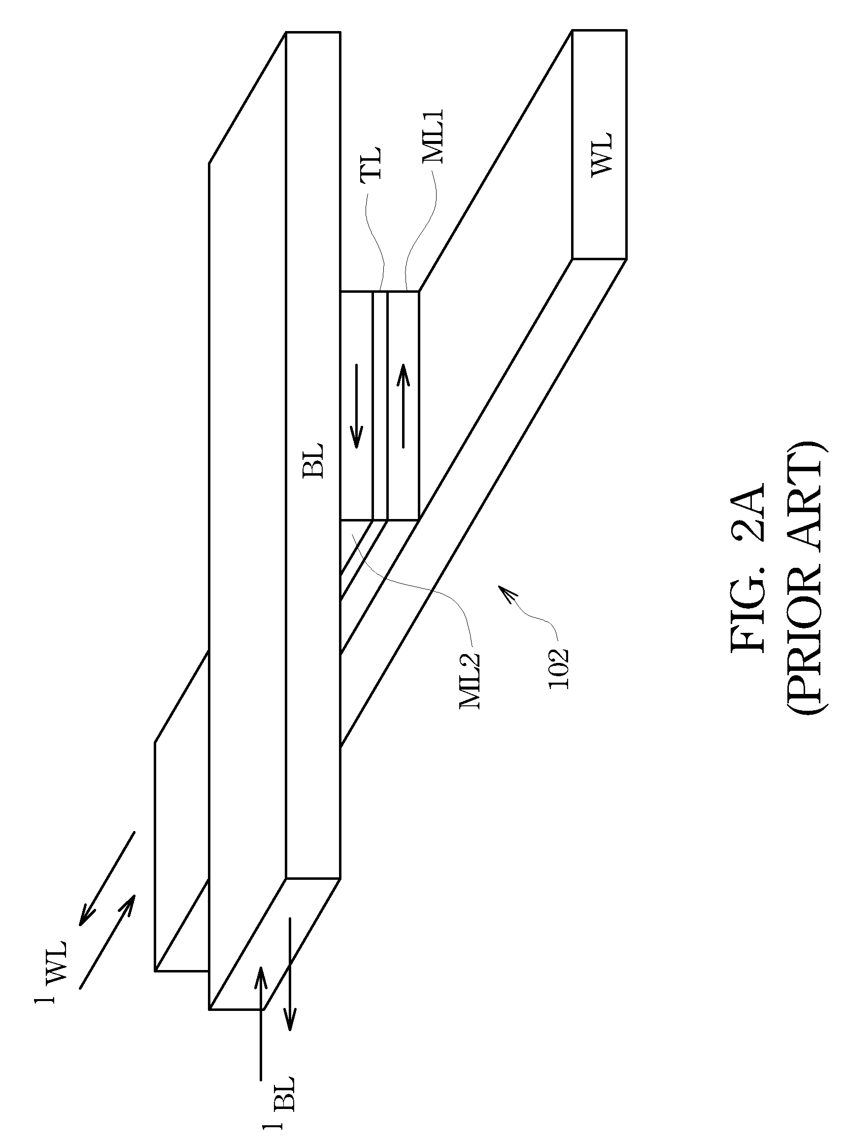
a technology of mtj and capping layer, which is applied in the field of magnetic resonance random access memory (mram) devices, can solve the problems of adversely affecting the performance of mtjs b>102, and the effect of inherent stresses of mtjs b>102/b> on their performance, and achieves the effect of substantially eliminating the adverse oxidation of mtj cells

Inactive Publication Date: 2009-08-20
TAIWAN SEMICON MFG CO LTD
View PDF8 Cites 126 Cited by
  • Summary
  • Abstract
  • Description
  • Claims
  • Application Information

AI Technical Summary

Benefits of technology

[0016]By forming a dielectric capping layer on MTJ cells before a vacuum break, the adverse oxidation of the MTJ cells is substantially eliminated.

Problems solved by technology

With the down-scaling of integrated circuits, the formation of MRAM devices experiences problems.
This adversely affects the performance of MTJs 102.
A further problem is the effect of inherent stresses in MTJs 102 to their performance.
The stresses may not be in a desirable direction, or have a desirable magnitude.
However, this cannot guarantee the reduction of the inherent stresses.

Method used


Image

  • In-Situ Formed Capping Layer in MTJ Devices
  • In-Situ Formed Capping Layer in MTJ Devices
  • In-Situ Formed Capping Layer in MTJ Devices

Examples


Embodiment Construction

[0023]The making and using of the presently preferred embodiments are discussed in detail below. It should be appreciated, however, that the present invention provides many applicable inventive concepts that can be embodied in a wide variety of specific contexts. The specific embodiments discussed are merely illustrative of specific ways to make and use the invention, and do not limit the scope of the invention.

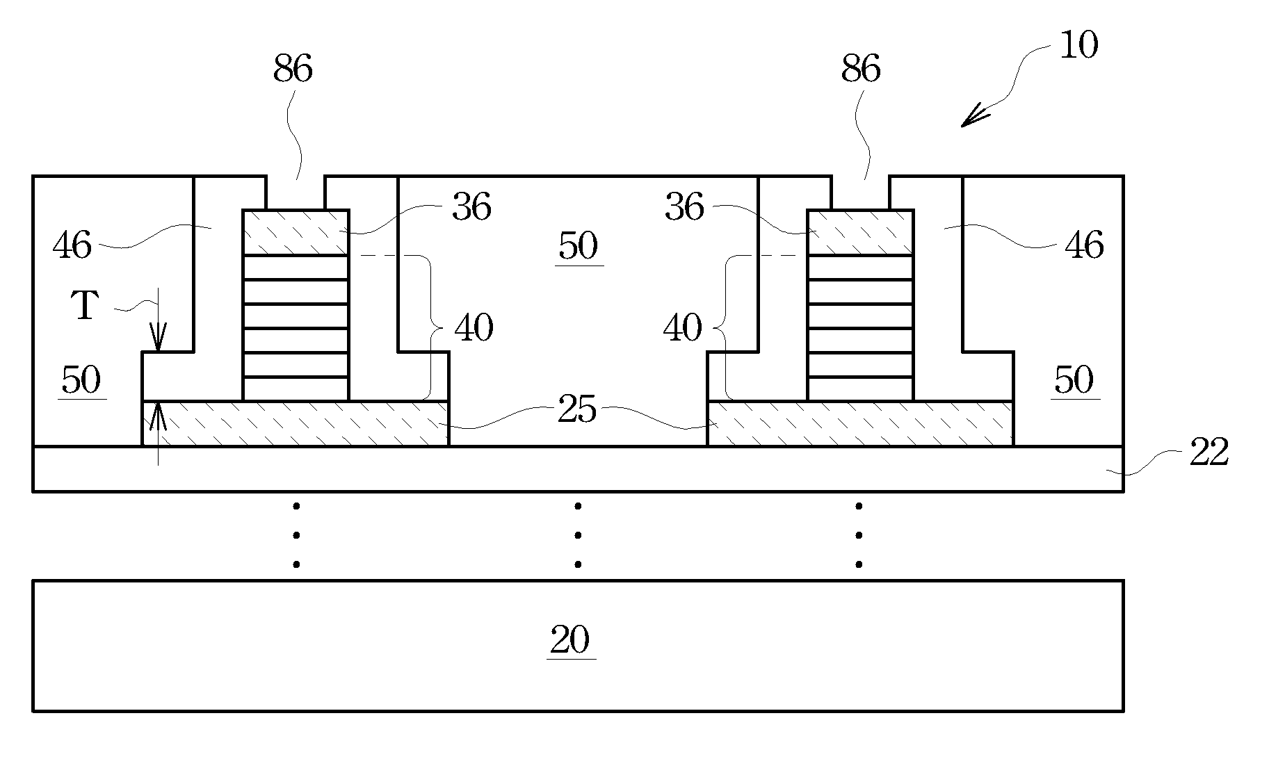
[0024]A novel magnetic tunnel junction (MTJ) and methods of forming the same are provided. The intermediate stages of manufacturing embodiments of the present invention are illustrated. Throughout the various views and illustrative embodiments of the present invention, like reference numbers are used to designate like elements.

[0025]FIG. 3 illustrates production tool 200 for forming the embodiments of the present invention. Production tool 200 includes transfer chamber 202 for transferring wafers, etching chambers 204 and 206 for etching components on the wafers, and depositi...


PUM


Abstract

A method of forming an integrated circuit includes forming magnetic tunnel junction (MTJ) layers; etching the MTJ layers to form a MTJ cell; and forming a dielectric capping layer on sidewalls of the MTJ cell, wherein the step of forming the dielectric capping layer is in-situ performed with the step of etching the MTJ layers.

Description

TECHNICAL FIELD[0001]The present invention relates generally to semiconductor memory devices, and more particularly to magnetoresistive random access memory (MRAM) devices and methods of manufacturing the same.BACKGROUND[0002]Semiconductors are used in integrated circuits for electronic applications, including radios, televisions, cell phones, and personal computing devices, as examples. One type of semiconductor device is the semiconductor storage device, such as dynamic random access memory (DRAM) or a flash memory, both of which use charge to store information.[0003]A more recent development in semiconductor memory devices involves spin electronics, which combines semiconductor technology and magnetic materials and devices. The spins of electrons, through their magnetic moments, rather than the charge of the electrons, is used to indicate the presence of a “1” or “0”. One such spin electronic device is a magnetoresistive random access memory (MRAM) device 100, sometimes referred ...

Claims


Application Information

Patent Timeline
Patent Type & Authority Applications(United States)
IPC IPC(8): H01L21/00
CPCH01L43/12H01L27/228G11C11/1659G11C11/161G11C11/1657H10B61/22H10N50/01H10N50/10
Inventor WANG, YUNG-HUNGWANG, YU-JENJUANG, MARKTSAI, CHIA-SHIUNG
Owner TAIWAN SEMICON MFG CO LTD
Why Eureka
Try Eureka