Multilayer interconnection substrate, semiconductor device, and solder resist

A multi-layer interconnection, semiconductor technology, applied in the direction of semiconductor devices, semiconductor/solid-state device manufacturing, semiconductor/solid-state device components, etc., can solve problems such as damage, large, damaged joints, etc. The effect of reducing inductance and elastic modulus

Inactive Publication Date: 2007-10-03
FUJITSU LTD
View PDF6 Cites 8 Cited by
  • Summary
  • Abstract
  • Description
  • Claims
  • Application Information

AI Technical Summary

Problems solved by technology

[0023] When the resin substrate with the semiconductor chip is warped, the junction between the resin substrate and the circuit substrate on which the semiconductor device with the resin substrate is mounted will act There is a large stress, which leads to the problem that the joint is damaged or damaged

Method used


Image

  • Multilayer interconnection substrate, semiconductor device, and solder resist
  • Multilayer interconnection substrate, semiconductor device, and solder resist
  • Multilayer interconnection substrate, semiconductor device, and solder resist

Examples


Embodiment Construction

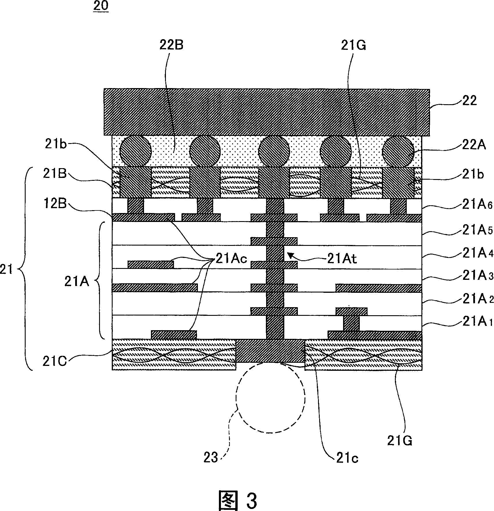
[0045] FIG. 3 shows the configuration of a semiconductor device 20 according to the first embodiment of the present invention.

[0046] 3, the semiconductor device 20 is formed by a resin multilayer interconnection substrate 21 and a semiconductor chip 22 flip-chip mounted on the resin multilayer interconnection substrate 21 through solder bumps 22A, wherein the resin multilayer interconnection substrate 21 is formed. The connecting substrate 21 includes a resin build-up layer 21A, and a plurality of build-up layers 21A are stacked in the resin build-up layer 21A. 1 -21A 6 , and solder resist layers 21B and 21C are respectively formed on the top surface and the bottom surface of the resin build-up layer 21A. The built-in layer 21A 1 -21A 6 Cu interconnection pattern 21Ac is formed on each layer of each layer. The Cu interconnection pattern 21Ac is, for example, a via pattern with a diameter of 40 μm and a line-and-space pattern of 30 μm / 30 μm in line width and line spacing....


PUM

PropertyMeasurementUnit
elastic modulusaaaaaaaaaa
thicknessaaaaaaaaaa
thicknessaaaaaaaaaa

Abstract

A multilayer interconnection substrate includes a resin laminated structure in which plural build-up layers are laminated, each of the plural build-up layers comprising an insulation layer and an interconnection pattern, and first and second solder resist layers provided on a top surface and a bottom surface of the resin laminated structure, wherein each of the first and second solder resist layers includes a glass cloth.

Description

technical field [0001] The present invention generally relates to semiconductor devices, and more particularly, to a resin material and a multilayer interconnection substrate using the resin material. Background technique [0002] Today's high-performance semiconductor devices use multilayer resin substrates as package substrates on which semiconductor chips are carried. [0003] On the other hand, a large amount of heat is generated in semiconductor chips used in high-performance semiconductor devices today, and thus warpage caused by thermal stress is liable to occur in the multilayer resin substrate carrying the semiconductor chips. It should be noted that the semiconductor chip has a larger elastic modulus than the resin substrate. [0004] In this way, when a semiconductor device is mounted on a circuit board through a solder bump or the like, a large amount of stress acts on the solder bump due to heat energy generated by the semiconductor device; space, or the elect...

Claims


Application Information

Patent Timeline
Patent Type & Authority Applications(China)
IPC IPC(8): H01L23/498H01L23/12H01L21/60H05K1/02
CPCH05K2201/029H05K3/281H01L23/49822H05K3/4644H01L2224/32225H01L23/4922H01L2924/15311H01L2224/73204H01L2924/01078H01L2224/73203H01L21/563H01L23/145H01L2224/16225H01L2924/00H05K3/46
Inventor 仓科守水谷大辅
Owner FUJITSU LTD
Why Eureka
Try Eureka