Capacitor compatible with high dielectric constant materials having a low contact resistance layer and the method for forming same

a capacitor and dielectric constant technology, applied in the field of semiconductor capacitors, can solve the problems of inability to simply deposit, incompatible high dielectric constant materials with existing processes, polysilicon electrodes, etc., and achieve the effect of maximizing the capacitance of the storage node and reducing the problem of high contact resistan

Inactive Publication Date: 2006-01-05
NANYA
View PDF43 Cites 9 Cited by
  • Summary
  • Abstract
  • Description
  • Claims
  • Application Information

AI Technical Summary

Benefits of technology

[0015] Since the barrier layer is protected during the formation of the dielectric layer by both the oxidation resistant conductive layer and the thick insulative

Problems solved by technology

Unfortunately high dielectric constant materials are incompatible with existing processes and can not be simply deposited on a polysilicon electrode as was the case for the lower dielectric constant materials, such as Si3N4 and SiO2/Si3N4 composite layers.
Also the capacitors employing the former materials undergo

Method used


Image

  • Capacitor compatible with high dielectric constant materials having a low contact resistance layer and the method for forming same
  • Capacitor compatible with high dielectric constant materials having a low contact resistance layer and the method for forming same
  • Capacitor compatible with high dielectric constant materials having a low contact resistance layer and the method for forming same

Examples


Embodiment Construction

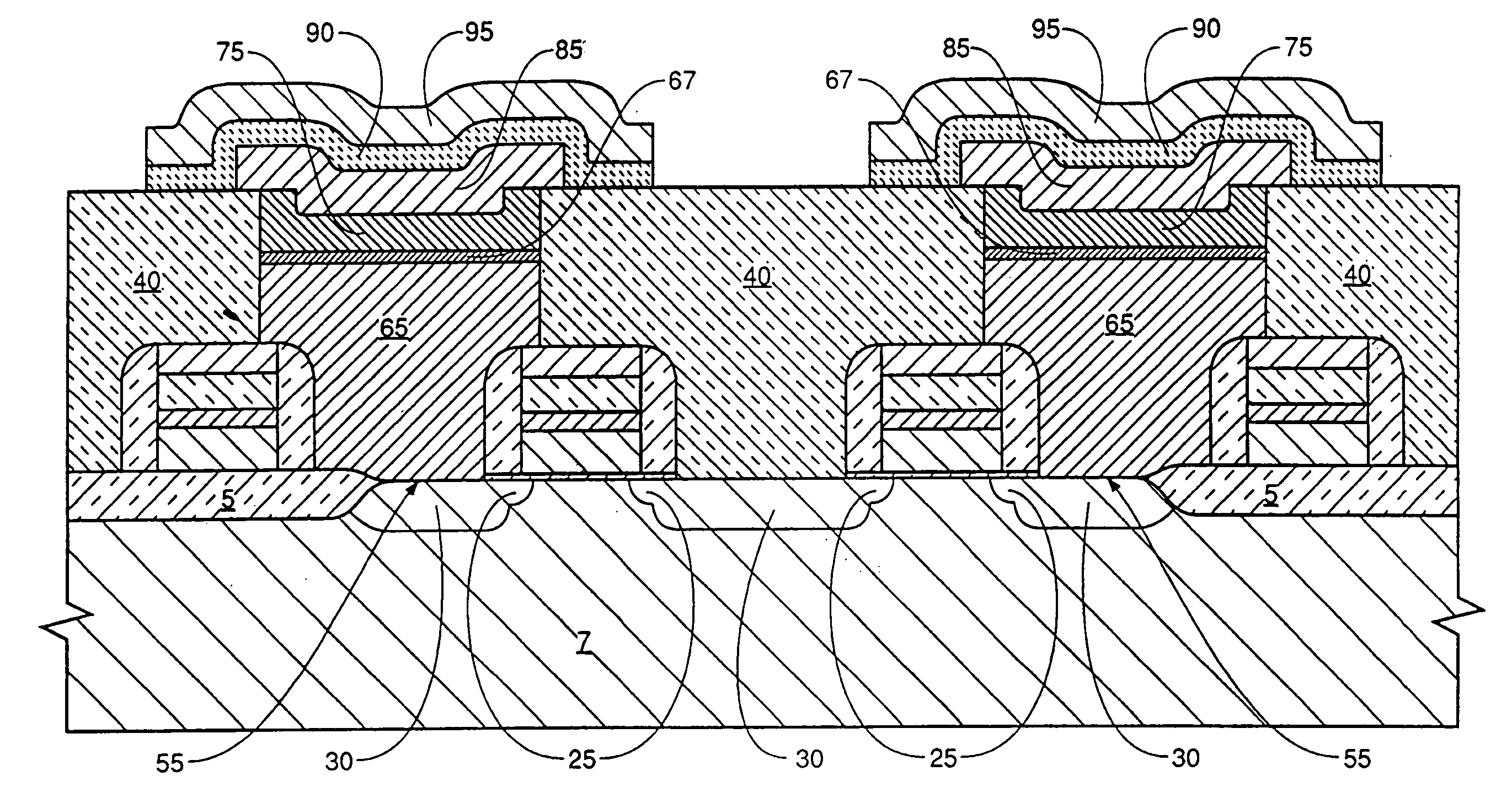
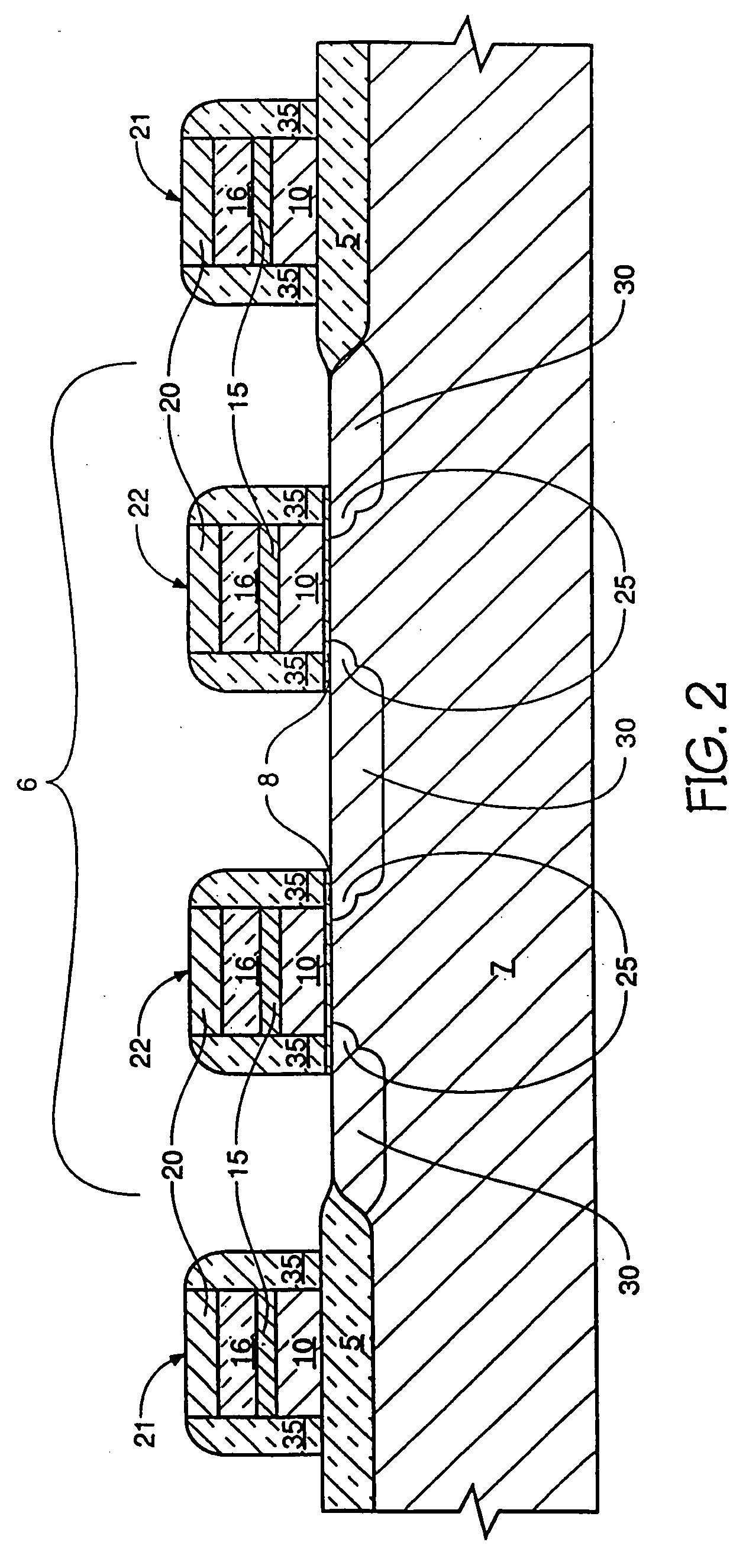
[0030] The method for fabricating the storage cell capacitor of the invention is shown pictorially in FIGS. 2-11.

[0031] Referring to FIG. 2, a cross-sectional view of an in-process dynamic random access memory (DRAM) cell is shown following conventional local oxidation of silicon (LOCOS) or special LOCOS processing which creates substantially planar field oxide regions 5 (created using modified LOCOS or trench isolation processes) and future active areas 6 (those regions of the substrate not covered by field oxide) on a silicon substrate 7. The creation of the field oxide is preceded or followed by a thermally grown dielectric layer 8 of silicon oxide. The depicted cell is one of many cells that are fabricated simultaneously and comprise a memory array. Following the creation of the field oxide region 5 and dielectric layer 8 a first conductively doped polysilicon layer 10, a metal silicide layer (Wsix) 15, an oxide layer 16, and a thick nitride layer 20 are deposited. The thick ni...


PUM


Abstract

A storage cell capacitor and a method for forming the storage cell capacitor having a storage node electrode including a barrier layer interposed between a conductive plug and an oxidation resistant layer. A layer of titanium silicide is fabricated to lie between the conductive plug and the oxidation resistant layer. An insulative layer protects the sidewalls of the barrier layer during the deposition and anneal of a dielectric layer having a high dielectric constant.

Description

RELATED APPLICATIONS [0001] This application is a Continuation of U.S. application Ser. No. 10 / 386,337, filed Mar. 10, 2003, which is a Divisional of U.S. Ser. No. 09 / 362,326, filed Jul. 27, 1999, now U.S. Pat. No. 6,531,730, which is a Continuation of U.S. Ser. No. 08 / 572,846, filed Dec. 14, 1995, now U.S. Pat. No. 5,959,327, which is a Continuation of U.S. Ser. No. 08 / 313,677, filed Sep. 27, 1994, now U.S. Pat. No. 5,506,166, which is a Divisional of U.S. Ser. No. 08 / 104,525, filed Aug. 10, 1993, now U.S. Pat. No. 5,381,302, which is a Continuation-In-Part of U.S. Ser. No. 08 / 044,331, filed on Apr. 2, 1993, and is a sister application to U.S. Ser. No. 08 / 104,524, filed Aug. 10, 1993, now U.S. Pat. No. 5,392,189, all of which are incorporated herein by reference.FIELD OF THE INVENTION [0002] This invention pertains to semiconductor technology, and more particularly to storage cell capacitors for use in dynamic random access memories. BACKGROUND OF THE INVENTION [0003] As memory dev...

Claims


Application Information

Patent Timeline
IPC IPC(8): H01L29/06H01L29/08H01L21/02H01L21/768H01L21/8242H01L21/8246H01L27/115
CPCH01L21/76846H01L21/76849H01L21/76855H01L21/7687H01L21/76895H01L28/75H01L27/10855H01L27/11502H01L27/11507H01L28/55H01L28/60H01L27/10852H10B12/033H10B12/0335H10B53/30H10B53/00
Inventor SANDHU, GURTEJ S.FAZAN, PIERRE C.
Owner NANYA
Why Eureka
Try Eureka