Projection lens arrangement

a technology of projection lens and projection lens, which is applied in the field of projection system, can solve the problems of reducing resolution, introducing distortion and reduction of resolution, and affecting the quality of beamlet control, and achieves uniform placement and dimensions

Active Publication Date: 2009-08-27
ASML NETHERLANDS BV
View PDF1 Cites 45 Cited by
  • Summary
  • Abstract
  • Description
  • Claims
  • Application Information

AI Technical Summary

Benefits of technology

[0007]The present invention seeks to improve the known systems and to address such problems by providing a charged particle multi-beamlet system for exposing a target using a plurality of beamlets. The system comprises a first plate having a plurality of holes formed in it, with a plurality of electrostatic projection lens systems formed at the location of each hole so that each electron beamlet passes through a corresponding projection lens system. The holes have sufficiently uniform placement and dimensions to enable focusing of the beamlets onto the surface of the target using a common control voltage.

Problems solved by technology

For high resolution lithography systems designed to operate at a commercially acceptable throughput, the size, complexity, and cost of such systems becomes an obstacle.
In this design, all the beamlets cross at a common cross-over, which introduces distortions and reduction of the resolution due to interactions between the charged particles in the beamlets.
However, when such a system is constructed having a large number of beamlets, providing multiple lenses for controlling each beamlet individually becomes impractical.
The construction of a large number of individually controlled lenses adds complexity to the system, and the pitch between the lenses must be sufficient to permit room for the necessary components for each lens and to permit access for individual control signals to each lens.
The greater height of the optical column of such a system results in several drawbacks, such as the increased volume of vacuum to be maintained and the long path for the beamlets which increases e.g. the effect of alignment errors caused by drift of the beamlets.

Method used


Image

  • Projection lens arrangement
  • Projection lens arrangement
  • Projection lens arrangement

Examples


Embodiment Construction

[0019]The following is a description of an embodiment of the invention, given by way of example only and with reference to the drawings.

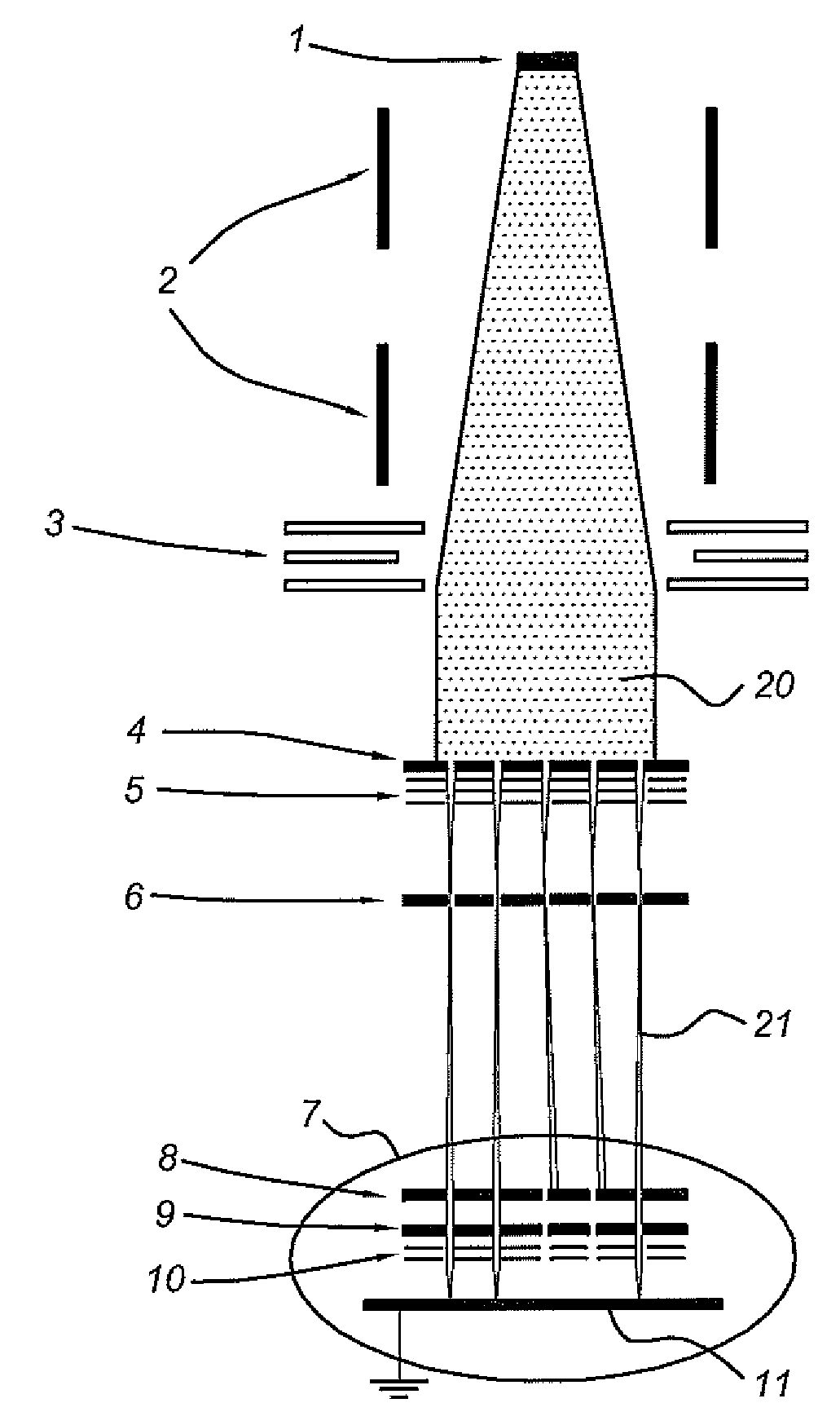
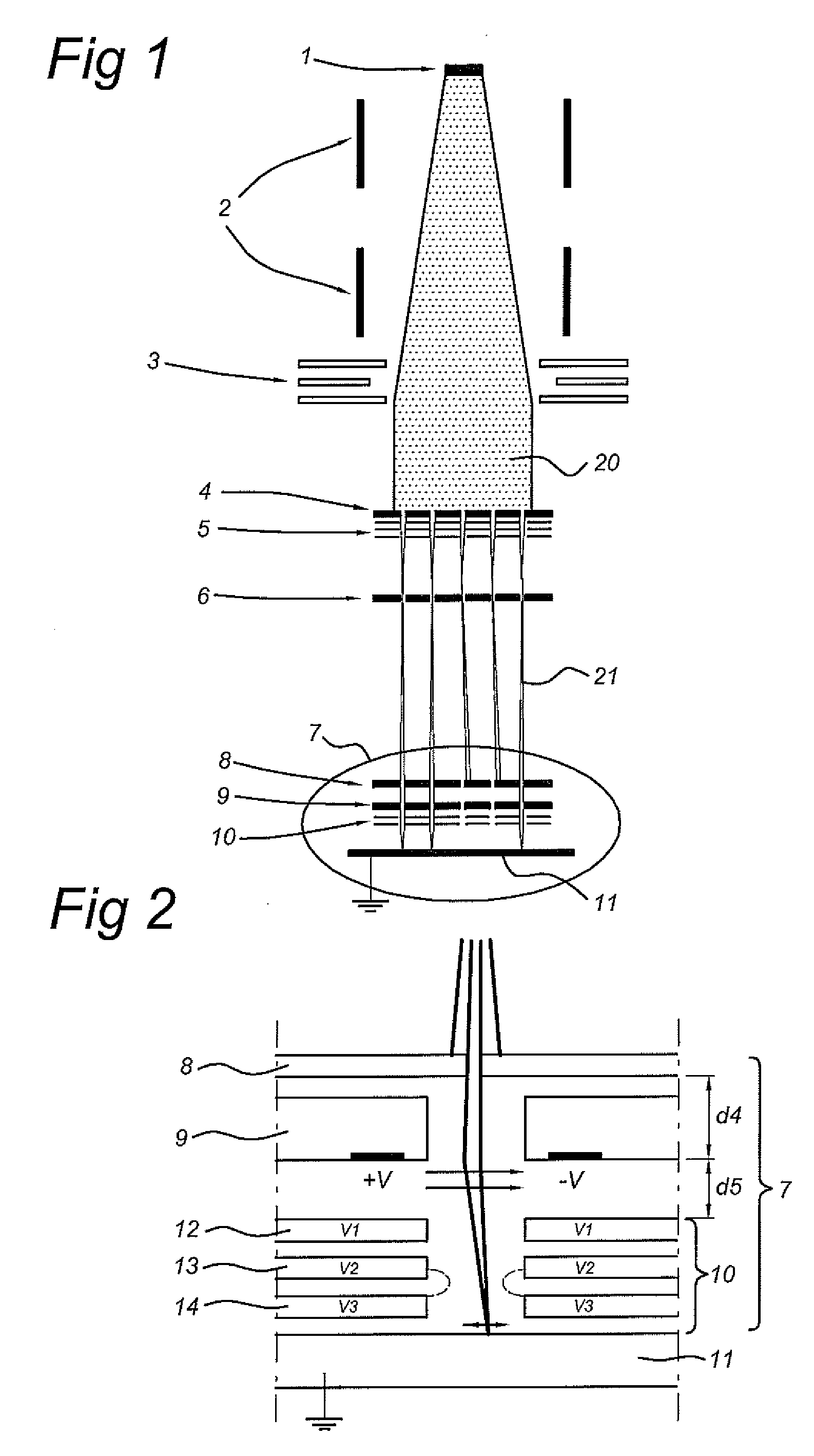
[0020]FIG. 1 shows a simplified schematic drawing of an embodiment of a charged particle multi-beamlet lithography system based upon an electron beam optical system without a common cross-over of all the electron beamlets. Such lithography systems are described for example in U.S. Pat. Nos. 6,897,458 and 6,958,804 and 7,084,414 and 7,129,502 which are all hereby incorporated by reference in their entirety, assigned to the owner if the present invention. In the embodiment shown in FIG. 1, the lithography system comprises an electron source 1 for producing a homogeneous, expanding electron beam 20. Beam energy is preferably maintained relatively low in the range of about 1 to 10 keV. To achieve this, the acceleration voltage is preferably low, the electron source preferably kept at between about −1 to −10 kV with respect to the target at ground potent...


PUM


Abstract

A charged particle multi-beamlet system for exposing a target using a plurality of beamlets. The system comprises a first plate having a plurality of holes formed in it, with a plurality of electrostatic projection lens systems formed at the location of each hole so that each electron beamlet passes through a corresponding projection lens system. The holes have sufficiently uniform placement and dimensions to enable focusing of the beamlets onto the surface of the target using a common control voltage. Preferably the electrostatic projection lens systems are controlled by a common electrical signal to focus the electron beamlets on the surface without correction of the focus or path of individual electron beamlets.

Description

BACKGROUND OF THE INVENTION[0001]1. Field of the Invention[0002]The present invention relates to a projection system for a charged particle multi-beamlet system, such as for a charged particle multi beamlet lithography system or an inspection system, and an end module for such a projection system.[0003]2. Description of the Related Art[0004]Currently, most commercial lithography systems use a mask as a means to store and reproduce the pattern data for exposing a target, such as a wafer with a coating of resist. In a maskless lithography system, beamlets of charged particles are used to write the pattern data onto the target. The beamlets are individually controlled, for example by individually switching them on and off, to generate the required pattern. For high resolution lithography systems designed to operate at a commercially acceptable throughput, the size, complexity, and cost of such systems becomes an obstacle.[0005]One type of design used for charged particle multi-beamlet ...

Claims


Application Information

Patent Timeline
Patent Type & Authority Applications(United States)
IPC IPC(8): H01J3/14A61N5/00G01J1/00
CPCB82Y10/00B82Y40/00H01J37/12H01J37/3007H01J2237/151H01J2237/0435H01J2237/1205H01J2237/121H01J37/3177
Inventor WIELAND, MARCO JAN JACOKAMPHERBEEK, BERT JANVAN VEEN, ALEXANDER HENDRIKKRUIT, PIETERSTEENBRINK, STIJN WILLEM HERMAN KAREL
Owner ASML NETHERLANDS BV
Why Eureka
Try Eureka