Fault Diagnosis of Serially-Addressed Memory Chips on a Test Adaptor Board To a Middle Memory-Module Slot on a PC Motherboard

a memory chip and serial-addressed technology, applied in error detection/correction, instruments, computing, etc., can solve problems such as packaging dram chips, wafer-sort tests may not catch all defects, and manufacturing defects to be somewhat common

Active Publication Date: 2009-08-27
KINGSTON DIGITAL CO LTD
View PDF1 Cites 22 Cited by
  • Summary
  • Abstract
  • Description
  • Claims
  • Application Information

AI Technical Summary

Problems solved by technology

The large number of memory cells, small size of individual memory cells, and overall large area of the DRAM die cause manufacturing defects to be somewhat common.
DRAM chips are tested on a wafer before being separated and packaged, but this wafer-sort test may not catch all defects.
Thus some packaged DRAM chips are going to contain defects.
However, when the memory chip under test is faulty, defect 56 may occur in the test program or in the OS image, causing the PC motherboard to crash.
Then the test program may crash, or it may report the failure.
However, when defect 56 in the memory modules device under test occurs in the portion of DRAM module slot 562 that contains the OS image, the PC motherboard is likely to crash during booting or just after booting.
This is less desirable, since the test program cannot report the location of the faulty memory.
Should a faulty DRAM location occur where the BIOS is loaded, the PC motherboard may crash during booting before the test program is executed.
This is undesirable since the exact location of defect 56 within the memory chip under test cannot be readily determined.
However, the test system can still detect the error by the motherboard crashing, and can discard the memory chip under test in test socket 560.

Method used


Image

  • Fault Diagnosis of Serially-Addressed Memory Chips on a Test Adaptor Board To a Middle Memory-Module Slot on a PC Motherboard
  • Fault Diagnosis of Serially-Addressed Memory Chips on a Test Adaptor Board To a Middle Memory-Module Slot on a PC Motherboard
  • Fault Diagnosis of Serially-Addressed Memory Chips on a Test Adaptor Board To a Middle Memory-Module Slot on a PC Motherboard

Examples


Embodiment Construction

[0036]The present invention relates to an improvement in memory chip testers and diagnosis tools. The following description is presented to enable one of ordinary skill in the art to make and use the invention as provided in the context of a particular application and its requirements. Various modifications to the preferred embodiment will be apparent to those with skill in the art, and the general principles defined herein may be applied to other embodiments. Therefore, the present invention is not intended to be limited to the particular embodiments shown and described, but is to be accorded the widest scope consistent with the principles and novel features herein disclosed.

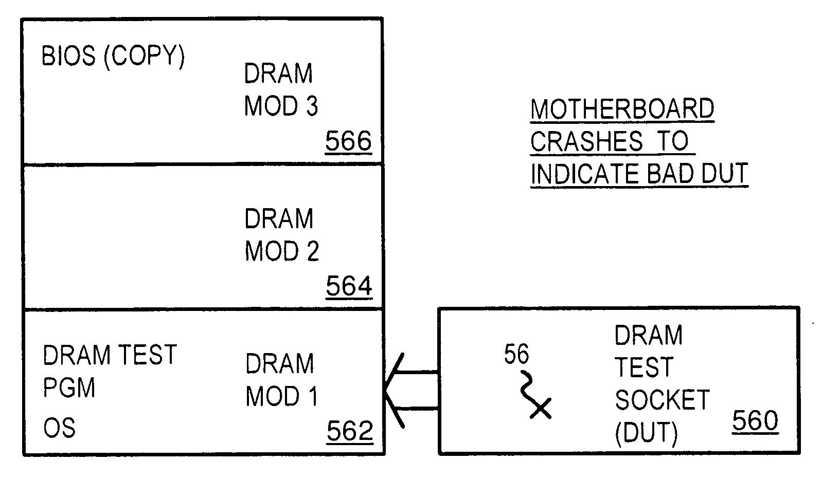
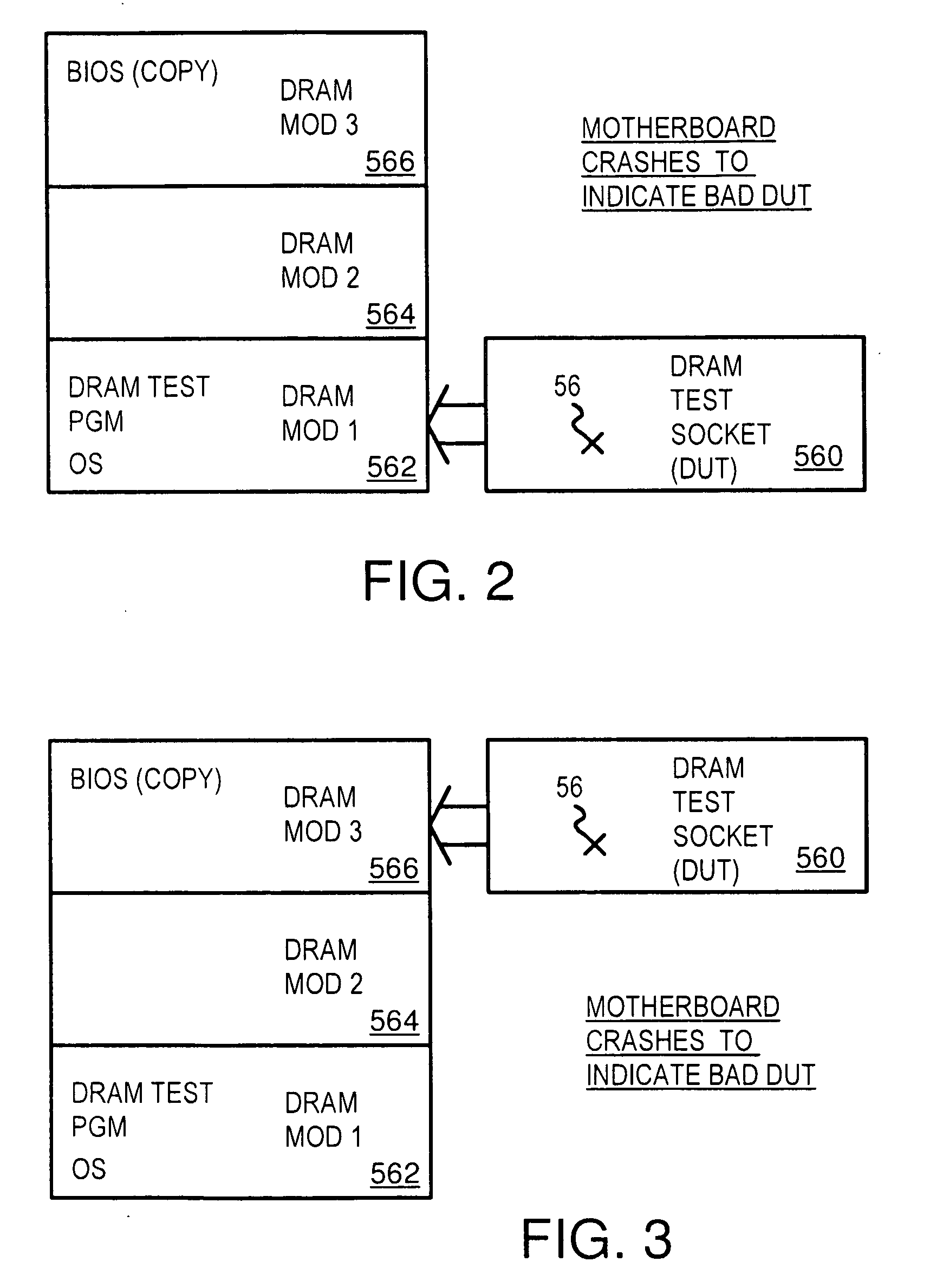
[0037]The inventor has realized that diagnosis of memory module failures can be aided by placing the memory chip under test in the middle of the motherboard's address space. Two good memory modules are inserted into standard memory module sockets on the motherboard, while a third memory module socket is removed...


PUM


Abstract

A standard memory module socket is removed from a target DRAM module slot on the component side and the test adaptor board connects to the target DRAM module slot on the reverse (solder) side of a personal computer motherboard, or an extender card may be used. The target DRAM module slot is a middle slot, such as the second or third of four DRAM module slots. The first and fourth DRAM module slots are populated with known good memory modules storing the BIOS at a high address and an operating system image and a test program at a low address. The test program accesses a memory chip in a test socket on a test adaptor board that is connected to the target DRAM module slot to locate defects. The motherboard does not crash since the BIOS, OS image, and test program are not stored in the memory chip under test.

Description

RELATED APPLICATIONS[0001]This application is a Continuation-In-Part (CIP) of U.S. Ser. No. 12 / 036,985, filed Feb. 25, 2008, and may be related to U.S. Ser. Nos. 10 / 249,841, 11 / 309,296, 11 / 309,297, 11 / 309,298, 11 / 944,551, and U.S. Pat. Nos. 7,277,337, 7,272,774, having a common assignee and at least one inventor in common, but presenting patentably distinct claims.FIELD OF THE INVENTION[0002]This invention relates to memory-chip testers, and more particularly to personal-computer motherboard-based memory testers.BACKGROUND OF THE INVENTION[0003]A wide variety of electronic systems use memory chips such as dynamic-random-access memory (DRAM). DRAM chips are often soldered to small daughter-cards to form memory modules. Personal computers (PC's) use memory modules as the main memory on the PC motherboard. Memory modules are built to meet specifications set by industry standards, thus ensuring a wide potential market. High-volume production and competition have driven module costs down...

Claims


Application Information

Patent Timeline
Patent Type & Authority Applications(United States)
IPC IPC(8): G06F11/00
CPCG11C5/04G11C29/56016G11C29/56008G11C29/56
Inventor CO, RAMON S.
Owner KINGSTON DIGITAL CO LTD
Why Eureka
Try Eureka