Image sensor and method to reduce dark current of CMOS image sensor

a technology of image sensor and cmos, which is applied in the field of image sensor, can solve the problems of reducing the quality of captured images, undesirable electrons, and limitation of the performance of such image sensors, and achieve the effect of reducing the dark current in image sensors

Inactive Publication Date: 2009-09-03
EASTMAN KODAK CO
View PDF5 Cites 29 Cited by
  • Summary
  • Abstract
  • Description
  • Claims
  • Application Information

AI Technical Summary

Benefits of technology

[0008]The present invention has the advantage of reducing dark current in image sensors.

Problems solved by technology

“Dark current” is a limitation of the performance of such image sensors.
These electrons are undesirable as they degrade the quality of the captured image.
Unfortunately, the light shield-silicon interface becomes a source of dark current.

Method used


Image

  • Image sensor and method to reduce dark current of CMOS image sensor
  • Image sensor and method to reduce dark current of CMOS image sensor
  • Image sensor and method to reduce dark current of CMOS image sensor

Examples


Embodiment Construction

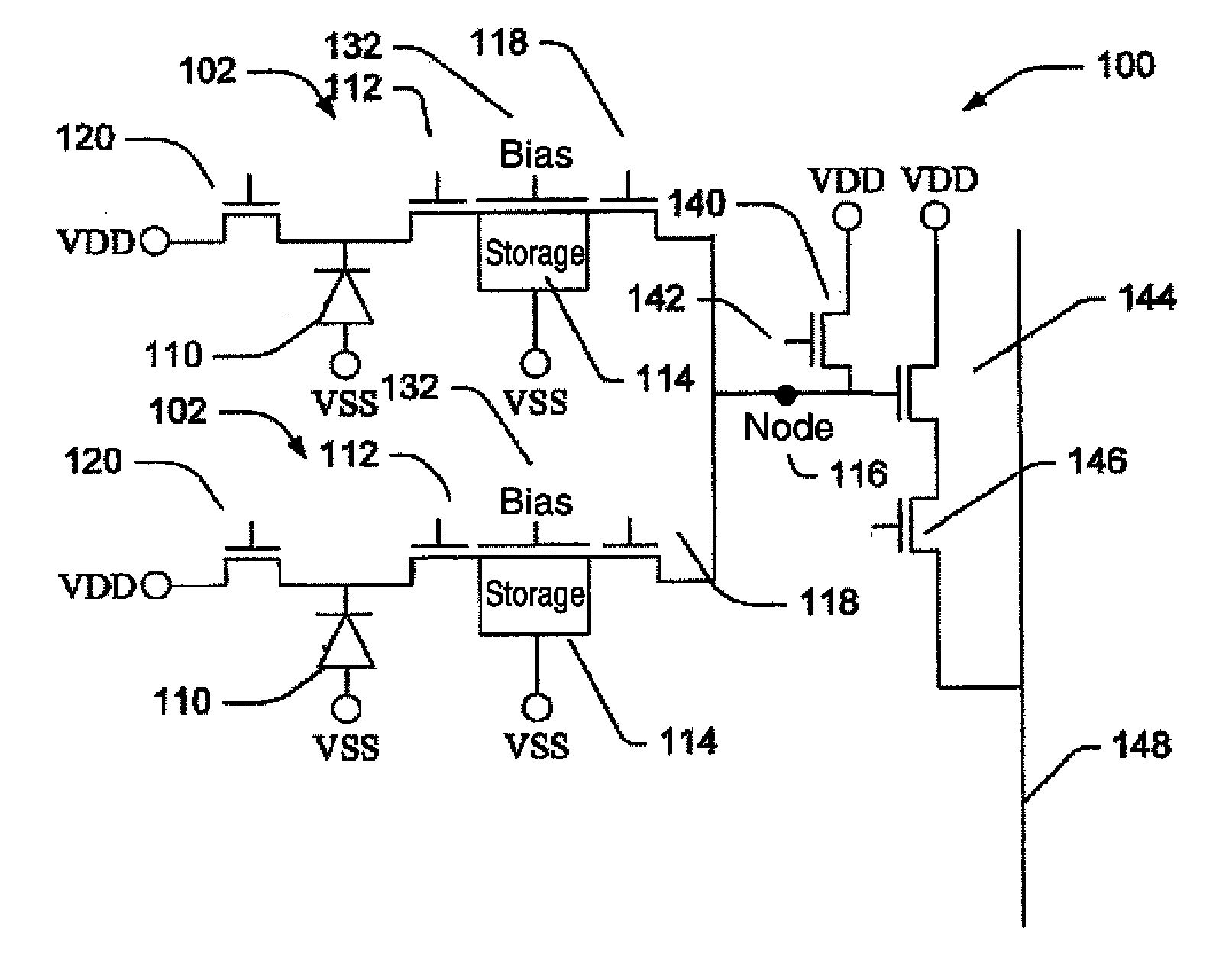
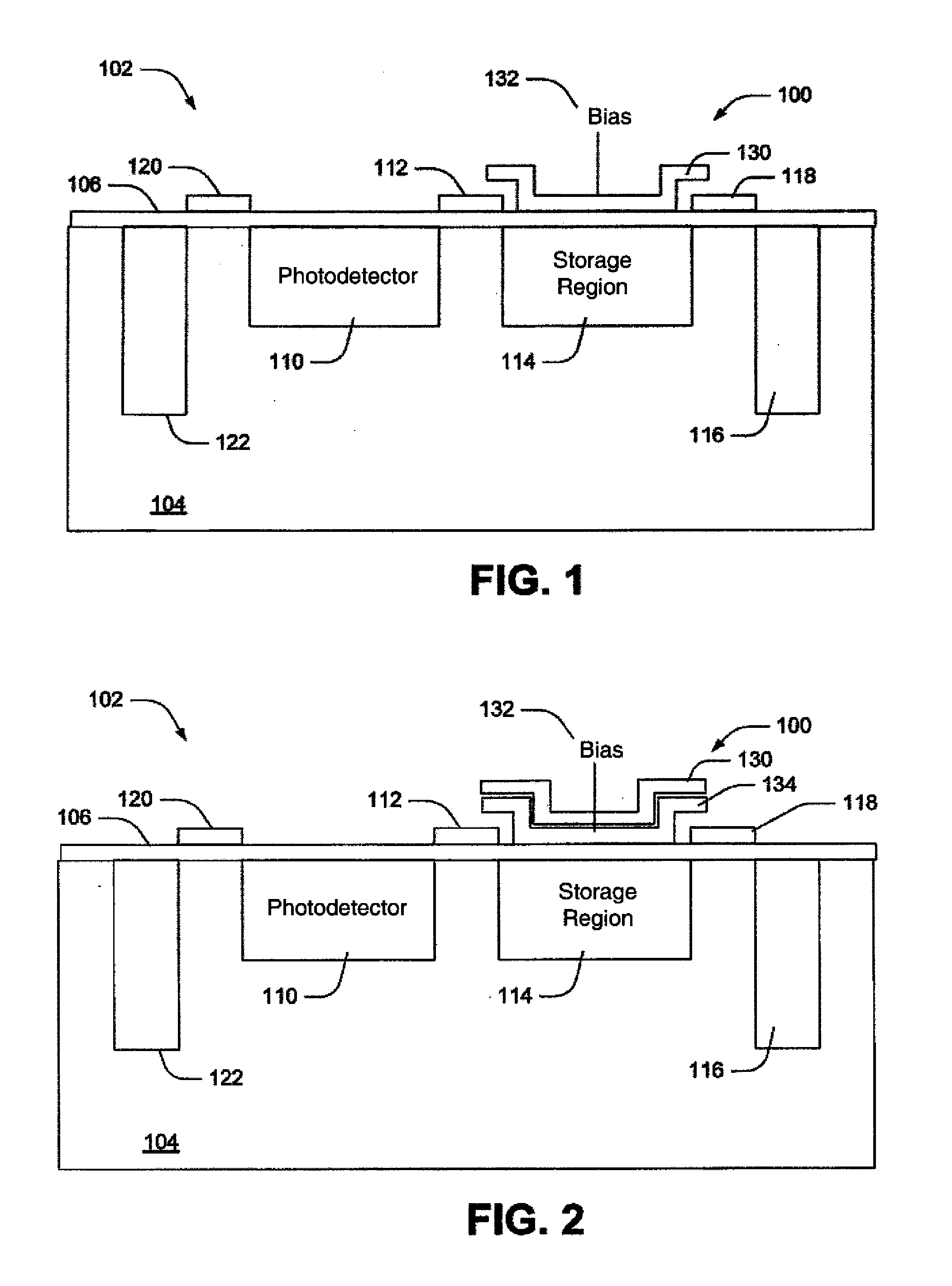
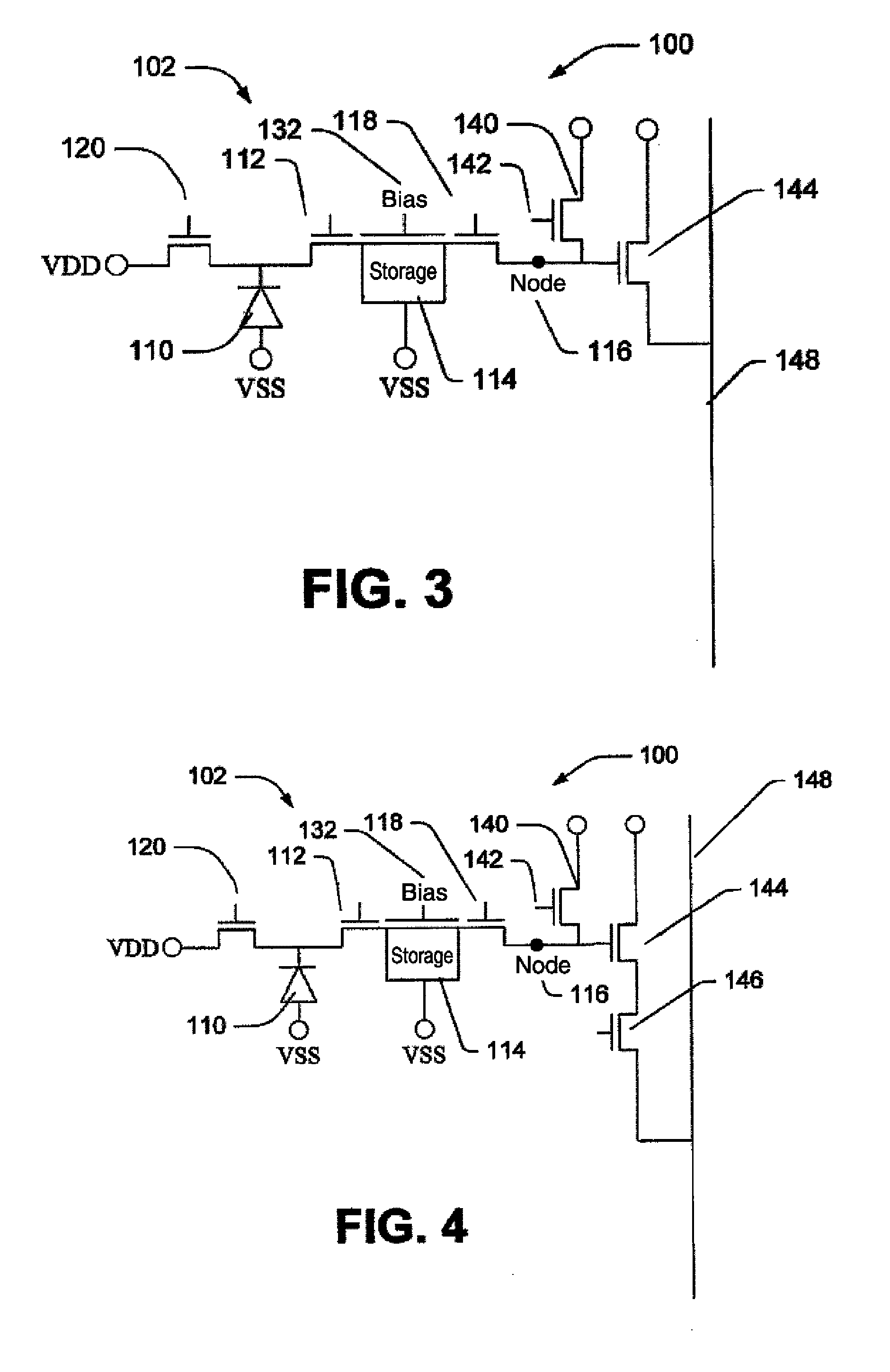
[0016]In the following Detailed Description, reference is made to the accompanying drawings, which form a part hereof, and in which is shown by way of illustration specific embodiments in which the invention may be practiced. In this regard, directional terminology, such as “top,”“bottom,”“front,”“back,”“leading,”“trailing,” etc., is used with reference to the orientation of the Figure(s) being described. Because components of embodiments of the present invention can be positioned in a number of different orientations, the directional terminology is used for purposes of illustration and is in no way limiting.

[0017]The meaning of “a,”“an,” and “the” includes plural reference, the meaning of “in” includes “in” and “on.” The term “connected” means either a direct electrical connection between the items connected or an indirect connection through one or more passive or active intermediary devices. The term “circuit” means either a single component or a multiplicity of components, either...


PUM


Abstract

An image sensor includes one or more photodetectors for collecting charge in response to incident light and a storage region adjacent each photodetector. A transfer mechanism transfers charge from each photodetector to a respective storage region. A conductive layer or a polysilicon layer is situated over each storage region. A bias voltage terminal is connected to each conductive layer or polysilicon layer for receiving a bias voltage to bias the conductive layer or polysilicon layer to a predetermined voltage level.

Description

FIELD OF THE INVENTION[0001]The invention relates generally to the field of image sensors, and more particularly, to reducing dark current in CMOS image sensors with global shutter.BACKGROUND OF THE INVENTION[0002]A typical image sensor includes a substrate having a photosensitive area or charge collection area for collecting charge, and a transfer gate for transferring charge from the photosensitive area to either a charge-to-voltage conversion mechanism, such as a floating diffusion in a CMOS image sensor, a transfer mechanism in a charge-coupled device image sensor or to a reset mechanism. A dielectric is positioned between the gate and the substrate, and the area of contact between the two areas is generally referred to as the semiconductor / dielectric interface.[0003]“Dark current” is a limitation of the performance of such image sensors. During certain stages of image capture, such as integration, electrons not associated with the photosensitive process that captures the electr...

Claims


Application Information

Patent Timeline
Patent Type & Authority Applications(United States)
IPC IPC(8): H04N5/217H01L27/146H04N5/361H04N5/374
CPCH01L27/14609H04N5/361H01L27/14812H01L27/14645H04N25/63
Inventor FUJITA, HIROAKI
Owner EASTMAN KODAK CO
Why Eureka
Try Eureka