Method For Manufacturing EL Display Device

a technology of el display device and manufacturing method, which is applied in the direction of electric lighting source, solid-state device, and light source, can solve the problems of difficult to further reduce achieve the reduction of the number of manufacturing steps of thin film transistors, and the reduction of the number of photomasks

Inactive Publication Date: 2009-09-10
SEMICON ENERGY LAB CO LTD
View PDF58 Cites 19 Cited by
  • Summary
  • Abstract
  • Description
  • Claims
  • Application Information

AI Technical Summary

Benefits of technology

[0037]It is not necessary that a photomask used for formation of a pattern of a gate electrode be newly formed, and thus, the number of manufacturing steps of a thin film transistor can be significantly reduced. Such a transistor can be applied to an EL display device. Therefore, the number of manufacturing steps of the EL display device can be significantly reduced.
[0038]More specifically, the number of photomasks can be reduced. It is possible to form a thin film transistor by using only one photomask (a multi-tone mask). Accordingly, the number of manufacturing steps of the EL display device can be significantly reduced.
[0039]Further, a complicated step such as backside light exposure, resist reflow a lift-off method, or the like is not needed unlike the conventional technique which is aimed at reducing the number of photomasks. Therefore, the number of manufacturing steps of the EL display device can be significantly reduced without reducing yield.
[0040]In the conventional technique, the number of photomasks is reduced at the cost of electric characteristics. However, in one embodiment of the invention, the number of manufacturing steps of a thin film transistor can be significantly reduced while keeping electric characteristics of the thin film transistor. Therefore, the number of manufacturing steps of an EL display device can be significantly reduced without degrading display quality and the like of the EL display device.
[0041]Furthermore, in accordance with the above effect, the manufacturing cost of the EL display device can be significantly reduced. Note that the thin film transistor manufactured by the method of one embodiment of the invention has a cavity adjacent to an end of a gate electrode layer; thus, leak current generated between a gate electrode and a drain electrode is small.

Problems solved by technology

However, even in the case where a bottom-gate thin film transistor is manufactured using the above multi-tone mask, at least two photomasks are required, and it is difficult to further reduce the number of photomasks.

Method used


Image

  • Method For Manufacturing EL Display Device
  • Method For Manufacturing EL Display Device
  • Method For Manufacturing EL Display Device

Examples


embodiment 1

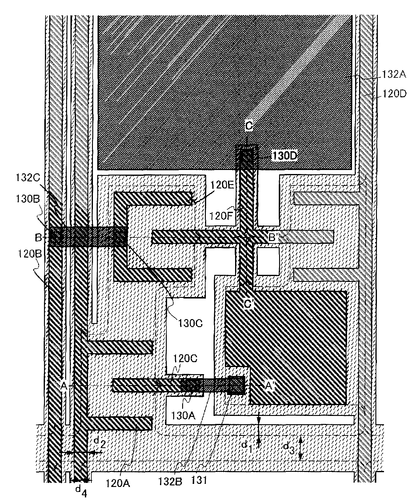
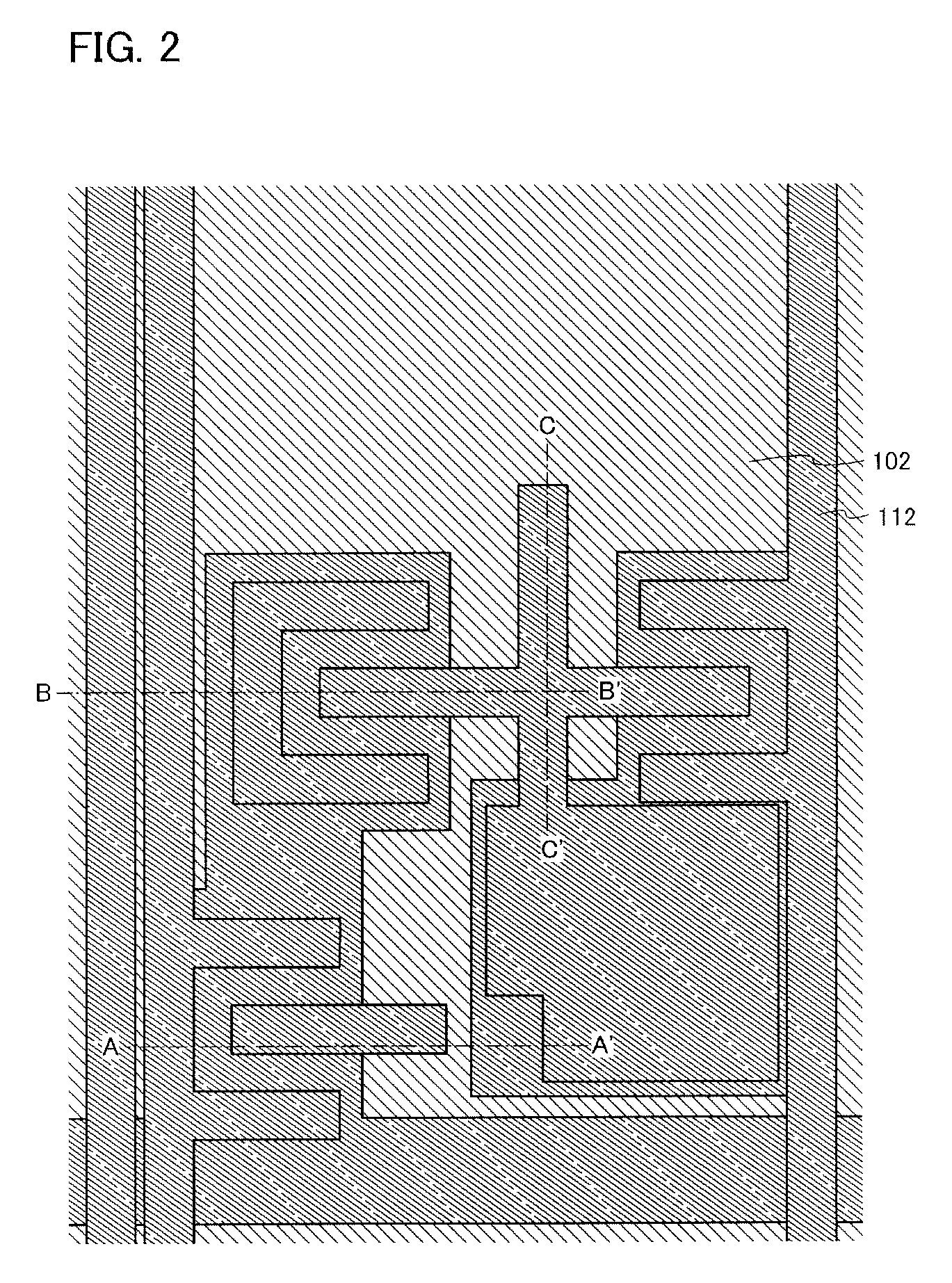
[0065]In this embodiment, an example of a method for manufacturing a thin film transistor and a method for manufacturing an EL display device in which the thin film transistors are arranged in matrix will be described with reference to FIGS. 1 to 16(B-2).

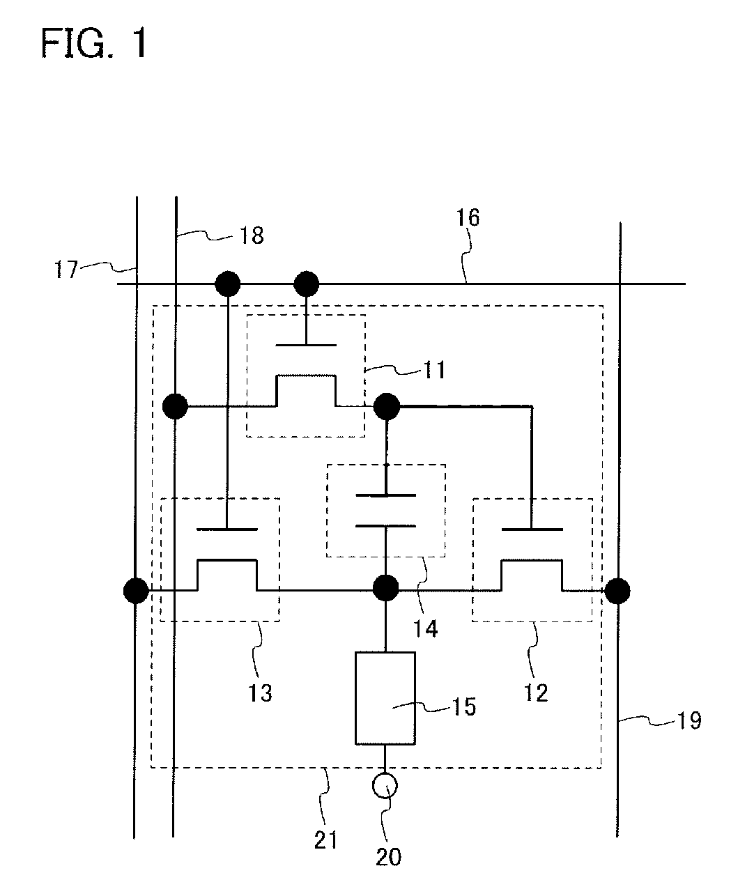
[0066]A variety of pixel circuits of an EL display device (an active EL display device) in which thin film transistors are used as switching elements are examined. In this embodiment, an example of a simple pixel circuit is illustrated in FIG. 1, and a manufacturing method of a pixel structure to which this pixel circuit is applied is described. However, a pixel circuit of an EL display device to be disclosed is not limited to the structure illustrated in FIG. 1.

[0067]In a pixel structure of an EL display device illustrated in FIG. 1, a pixel 21 includes a first transistor 11, a second transistor 12, a third transistor 13, a capacitor 14, and a light-emitting element 15. Each of the first to third transistors is an n-channel transis...

embodiment 2

[0179]In this embodiment, electronic appliances in which a display panel or a display device manufactured by a method described in Embodiment 1 is incorporated as a display portion will be described with reference to FIGS. 20A and 20B, FIG. 21, and FIGS. 22A to 22C. As such electronic appliances, for example, cameras such as video cameras and digital cameras, displays that can be mounted on a person's head (goggle-type displays), car navigation systems, projectors, car stereos, personal computers, and portable information terminals (e.g., mobile computers, mobile phones, and electronic books) can be given. Examples thereof are illustrated in FIGS. 20A and 20B.

[0180]FIG. 20A illustrates a television device. The television device illustrated in FIG. 20A can be completed by incorporating an EL display panel in a chassis. A main screen 223 is formed using a display panel manufactured according to the method described in Embodiment 1. In addition, a speaker portion 229, operation switche...


PUM


Abstract

A manufacture process of a thin film transistor mounted on an EL display device is simplified. A thin film transistor is manufactured by stacking a first conductive film, an insulating film, a semiconductor film, an impurity semiconductor film, and a second conductive film; forming a first resist mask over the stacked films; performing first etching to form a thin-film stack body; performing second etching by side etching is conducted on the thin-film stack body to form a gate electrode layer; and forming a source and drain electrode layer and the like with use of a second resist mask. An EL display device is manufactured using the thin film transistor.

Description

BACKGROUND OF THE INVENTION[0001]1. Field of the Invention[0002]The present invention relates to a method for manufacturing an EL display device which includes thin film transistors.[0003]2. Description of the Related Art[0004]In recent years, thin film transistors each of which are formed using a semiconductor thin film with a thickness of several nanometers to several hundreds of nanometers over a substrate having an insulating surface such as a glass substrate have attracted attention. Such thin film transistors are widely used for ICs (integrated circuits) and electronic devices such as electrooptic devices. In particular, rapid development of thin film transistors as switching elements of image display devices typified by liquid crystal display devices, EL (electro luminescence) display devices, and the like has been demanded.[0005]In an active matrix EL display device, voltage is applied between a pair of electrodes of a light-emitting element provided in a selected pixel, whi...

Claims


Application Information

Patent Timeline
Patent Type & Authority Applications(United States)
IPC IPC(8): H01L29/04H01L21/00H05B44/00
CPCH01L27/1214H01L27/1288H01L27/3262H10K59/1213H01L2924/13069H10K71/16H10K50/11
Inventor MIYAIRI, HIDEKAZUKOMORI, SHIGEKIISA, TOSHIYUKIUMEZAKI, ATSUSHI
Owner SEMICON ENERGY LAB CO LTD
Why Eureka
Try Eureka