

High density synapse chip using nanoparticles
a nanoparticle and high density technology, applied in the field of nanotechnology, can solve the problems of slow software simulation, unsuitable for many real-time problems of conventional computers, and proved extremely difficult, and achieve the effect of strengthening or weakening nanoconnections
- Summary
- Abstract
- Description
- Claims
- Application Information
AI Technical Summary
Benefits of technology
Problems solved by technology
Method used
Image

Examples
Embodiment Construction
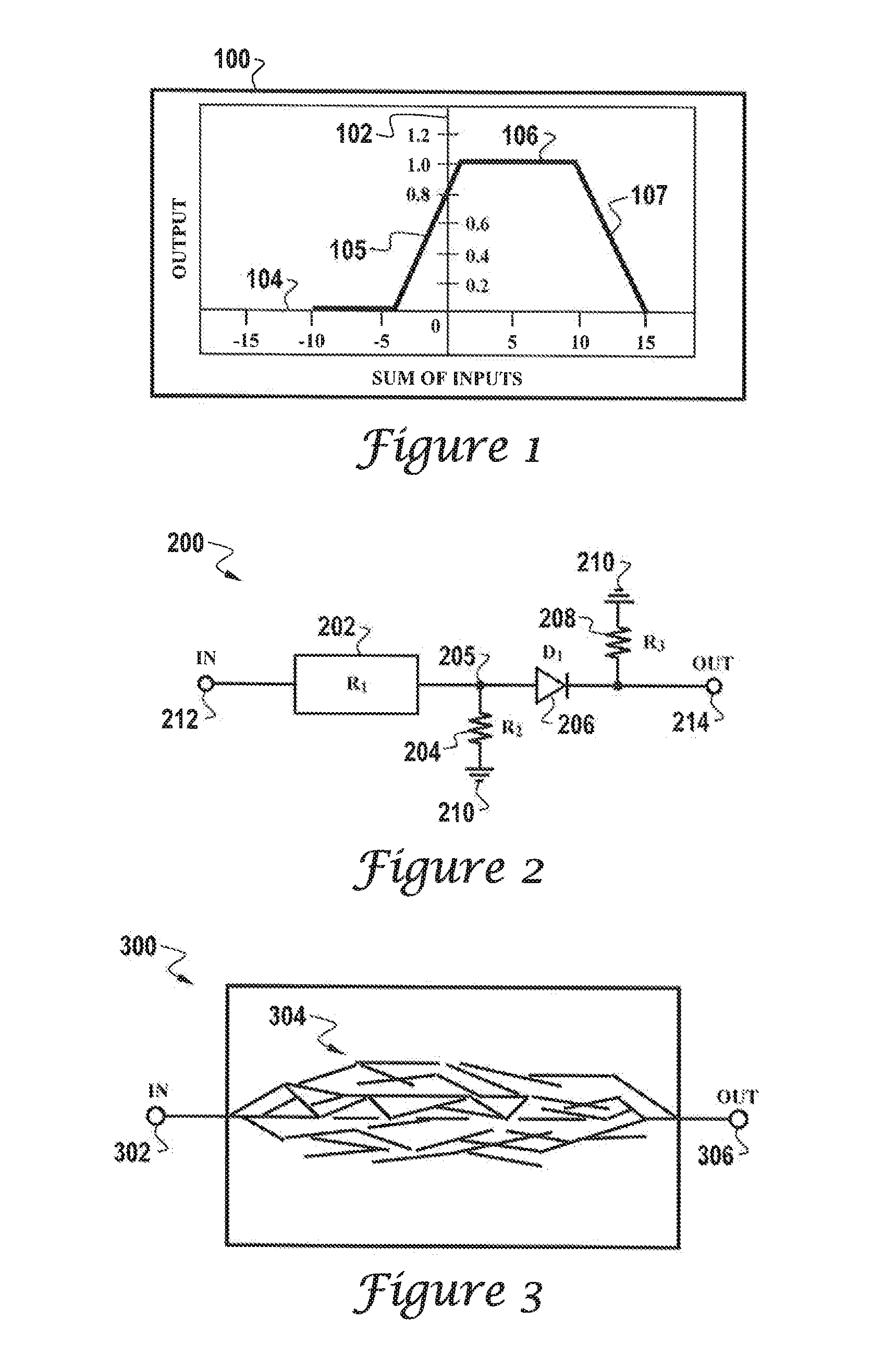
[0054]The particular values and configurations discussed in these non-limiting examples can be varied and are cited merely to illustrate an embodiment of the present invention and are not intended to limit the scope of the invention.
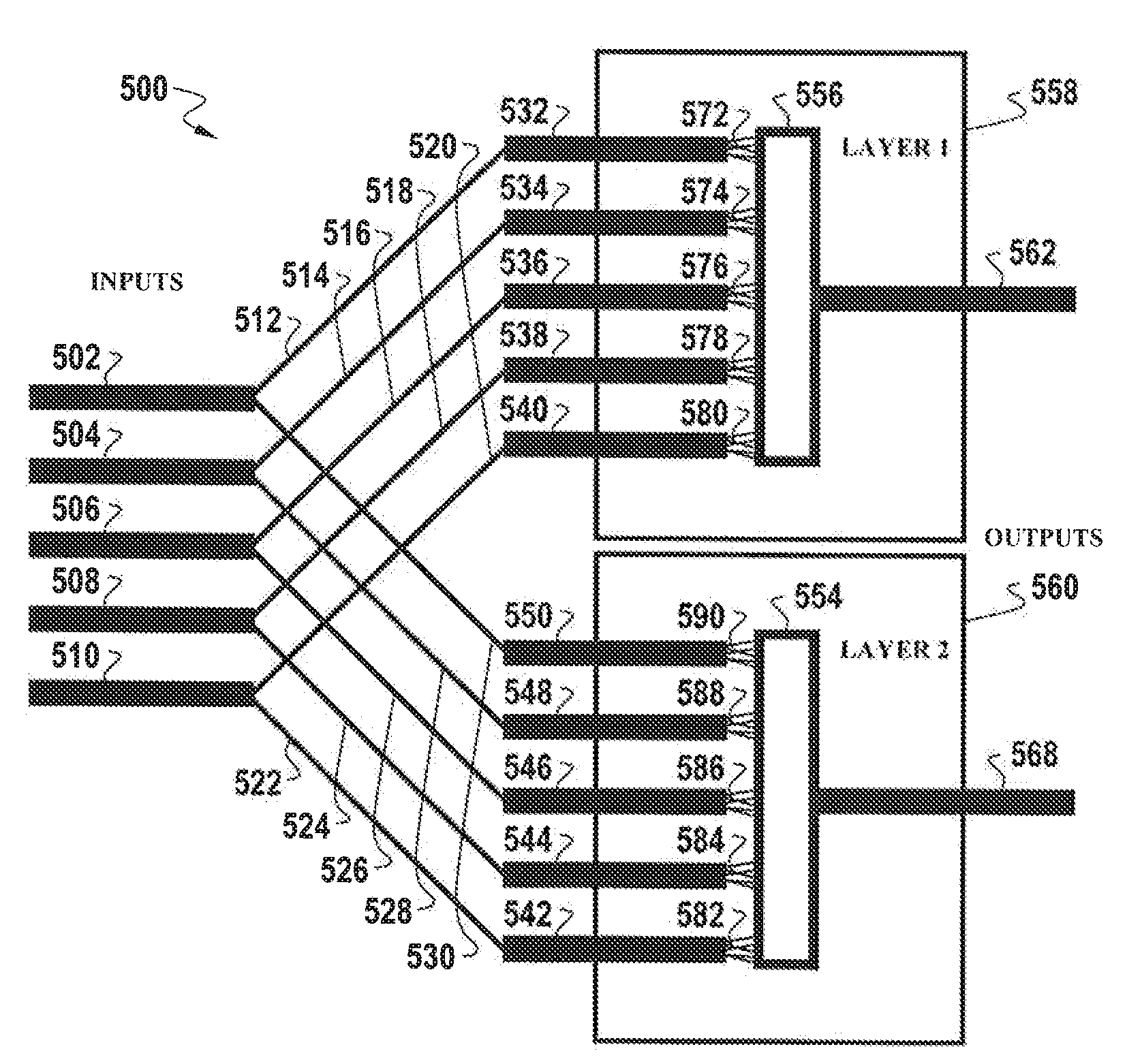
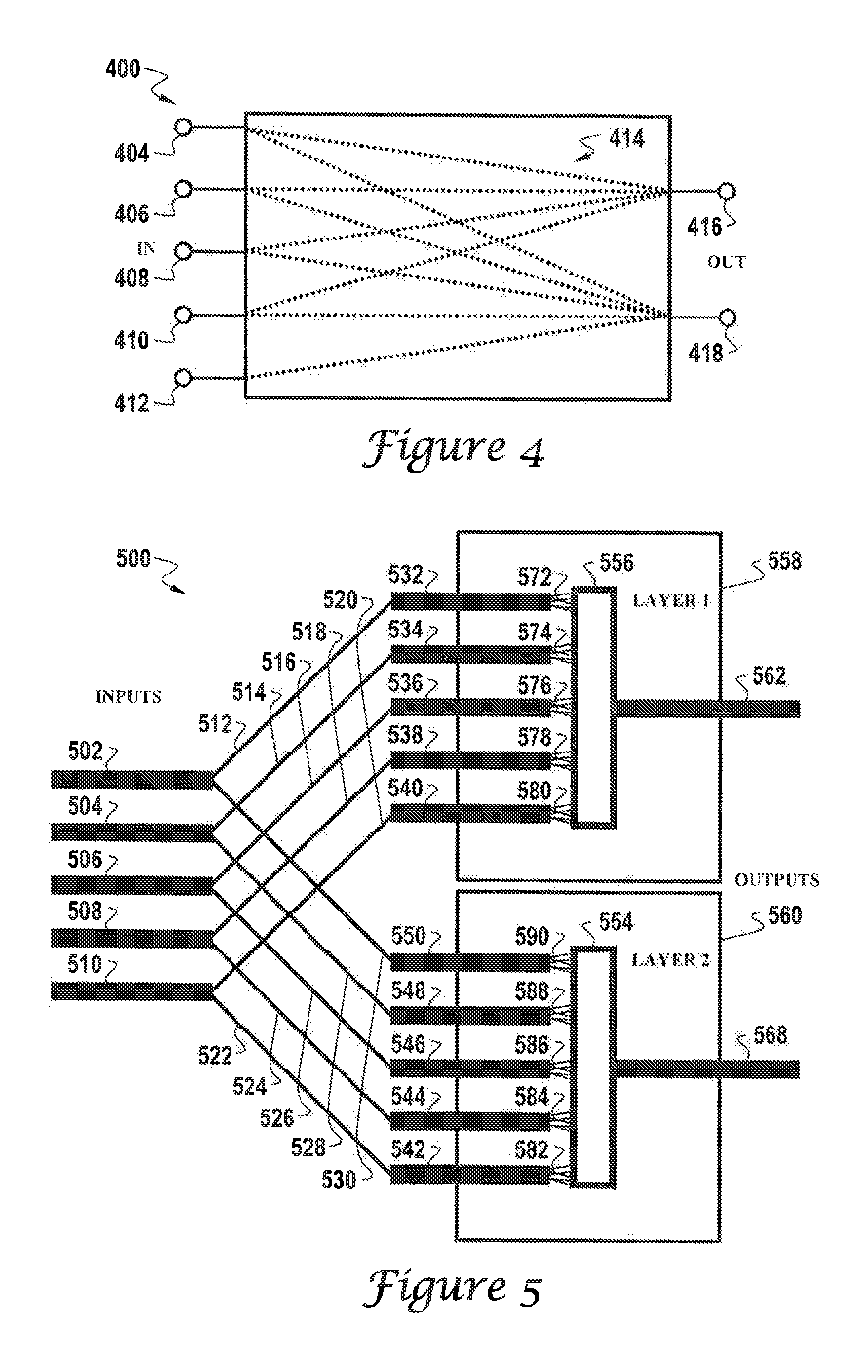
[0055]The physical neural network described and disclosed herein is different from prior art forms of neural networks in that the disclosed physical neural network does not require computer calculations for training, nor is its architecture based on any current neural network hardware device. The design of the physical neural network of the present invention is actually quite “organic”. The physical neural network described herein is generally fast and adaptable, no matter how large such a physical neural network becomes. The physical neural network described herein can be referred to generically as a Knowm™. The terms “physical neural network” and “Knowm” can thus be utilized interchangeably to refer to the same device, network, or structure. The term “...
PUM
 Abstract
Description
Claims
Application Information