Plasma etching method

a technology of etching method and plasma, which is applied in the direction of basic electric elements, electrical equipment, semiconductor devices, etc., can solve the problems of gate depletion, increase of leak current, and increase of threshold voltage, and achieve the effect of large etching selection ratio

Active Publication Date: 2009-09-17
TOKYO ELECTRON LTD
View PDF3 Cites 8 Cited by
  • Summary
  • Abstract
  • Description
  • Claims
  • Application Information

AI Technical Summary

Benefits of technology

[0014]The present invention has been made in view of the above circumstances. The object of the present invention is to provide a plasma etching method for plasma-etching a metal nitride film and a silicon film which are side-by-side arranged, the plasma etching method being capable of achieving a large etching selection ratio of the metal nitride film relative to the silicon film, while a verticality of the etching process can be suitably maintained.
[0016]According to the present invention, in the etching method for etching the surface of the substrate in which the metal nitride film and the silicon film have been respectively formed on the first base film and the second base film that had been side-by-side arranged, with the surfaces of the metal nitride film and the silicon film being exposed, the plasma of the gas containing nitrogen is supplied onto the surface of the plasma so as to nitride the silicon film. Thus, hardness of the silicon film is increased, whereby the silicon film becomes hard to be etched. On the other hand, since the metal nitride film contains a large amount of nitrogen from the first, the metal nitride film is not nitrided. Thus, an etching selection ratio of the metal nitride film relative to the silicon film is increased. Accordingly, after the above nitriding process, when the metal nitride film and the silicon film are etched until the first base film is exposed, the silicon film can remain as a remaining film of a large thickness. For this reason, the remaining film of the silicon film can be efficiently etched in the succeeding step, by using the plasma of a process gas that is selected such that a selection ratio of the silicon film relative to the second base film is large, and that the first base film is not etched. As a result, a desired recess of a suitable shape can be formed, as well as a film-thickness-decrease of the second base film can be effectively restrained.

Problems solved by technology

However, when the thickness of the silicon oxide film is narrowed, an amount of leak current is increased.
However, when this type of high-dielectric-constant film is used as a gate insulation film, a problem such as a carrier fixation and / or a gate depletion may occur, which raises a threshold voltage in a transistor.
Herein, when metal gate films are applied to both a p-type transistor and an n-type transistor in one substrate, the metal gate films for the respective transistors have to be made of different materials, which complicates a manufacturing process.
However, when a chlorinated gas is used, it is impossible to achieve a large selection ratio of the metal gate film 105 relative to the polysilicon film 112.
When the process conditions for the etching process are adjusted so as to achieve a large selection ratio, as shown in FIG. 6B, a verticality of the etching process is likely to be deteriorated.
Therefore, adjustment range of the process conditions for achieving the large selection ratio is considerably narrow, and thus it is difficult to achieve the large selection ratio in practice.
However, the above problems are not considered at all.

Method used


Image

  • Plasma etching method
  • Plasma etching method
  • Plasma etching method

Examples


example

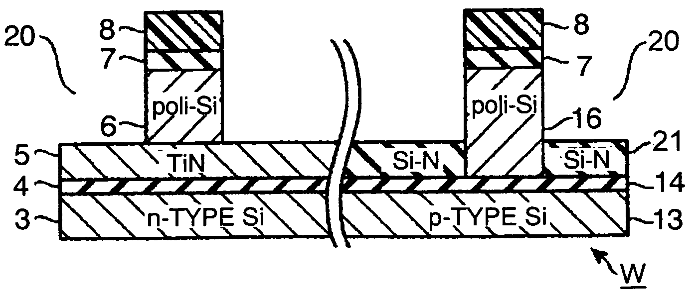
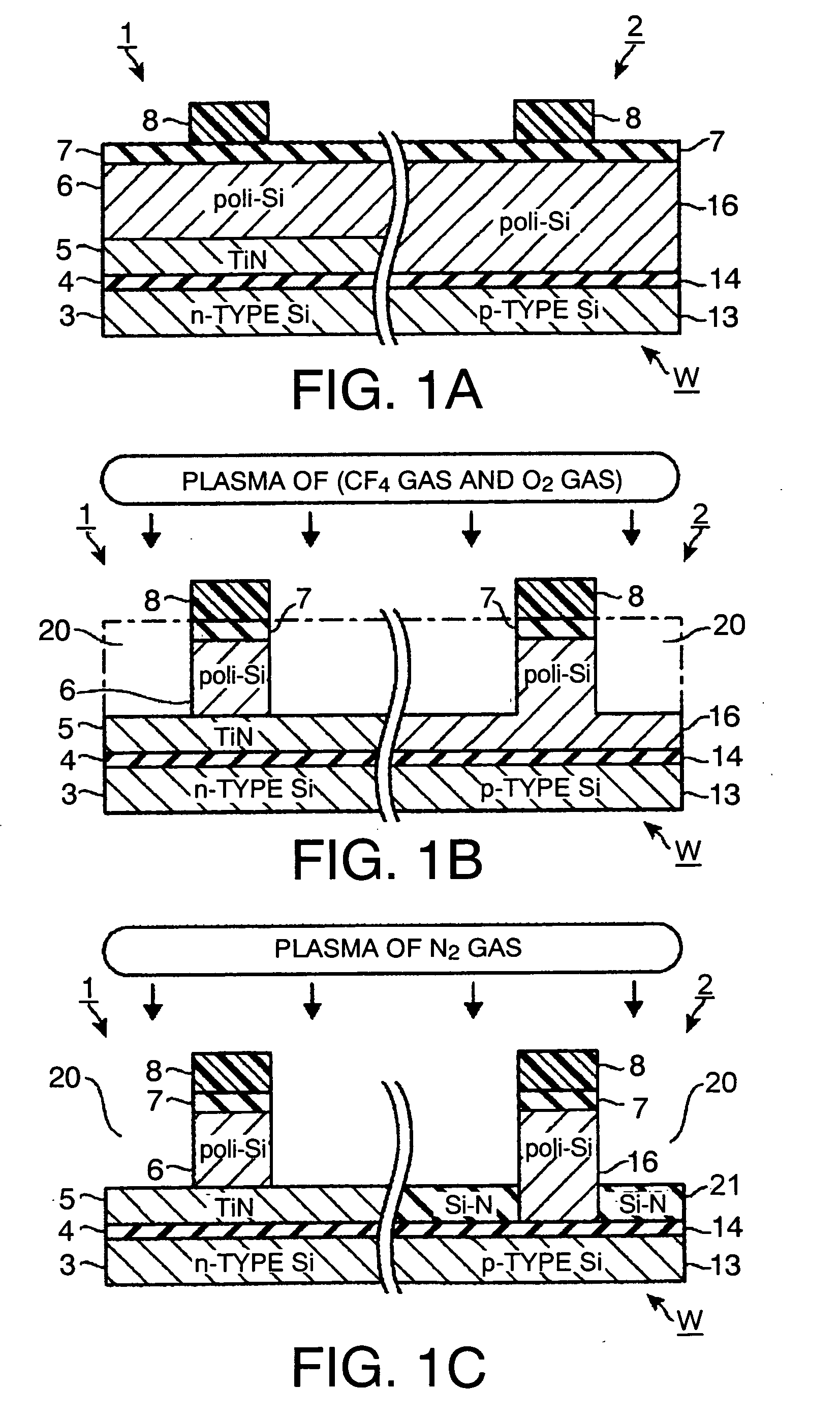
[0063]Next, an experiment conducted for confirming the effect of the present invention is described. In the experiment, two wafers W, each having the structure shown in FIG. 1A, were etched by the aforementioned plasma etching apparatus up to the upper end surfaces of the titanium nitride films 5.

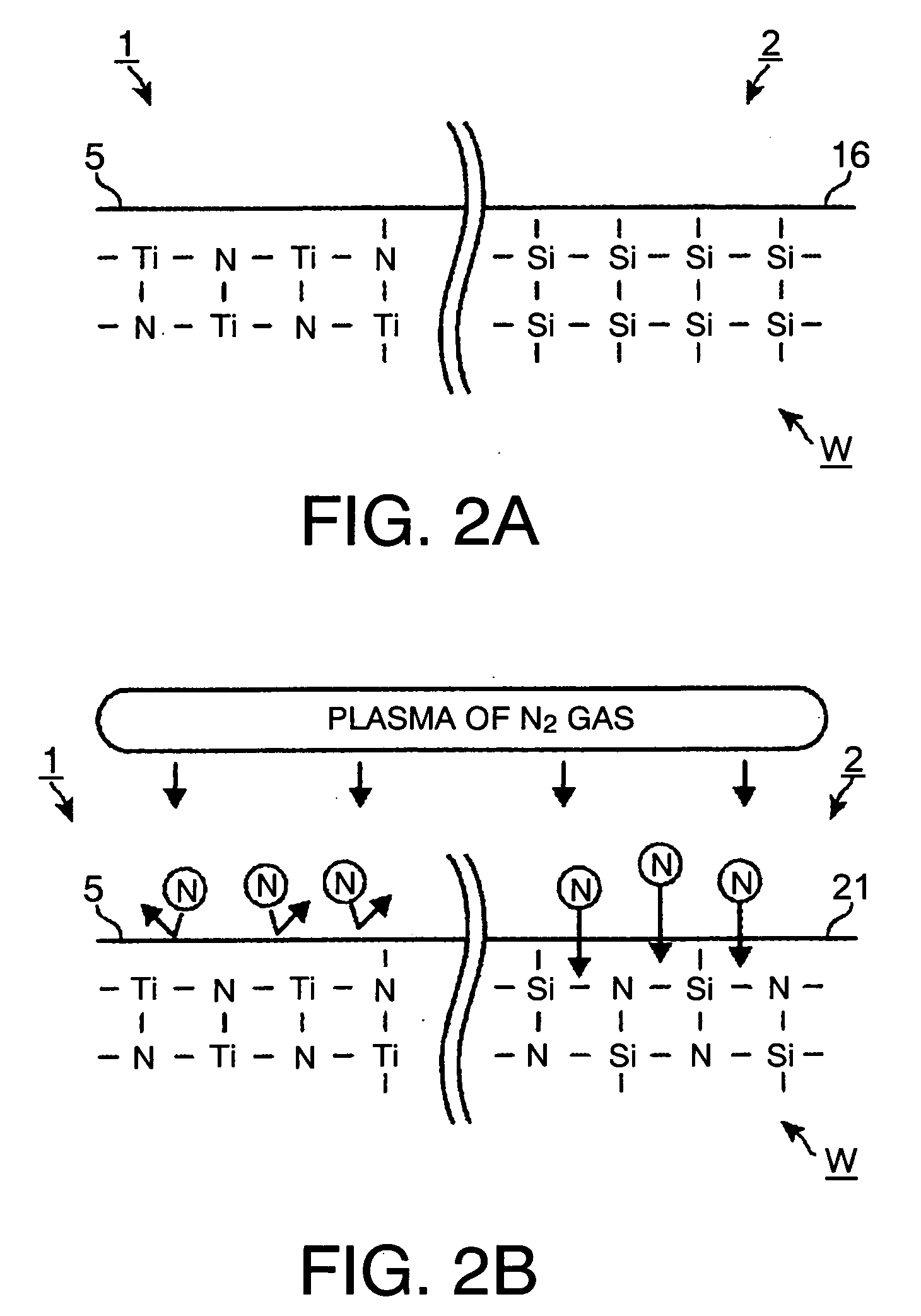
[0064]Thereafter, one wafer W was subjected to a nitriding process, which was performed under the conditions shown below. The other wafer W was not subjected to the nitriding process.

[0065]Following thereto, the titanium nitride films 5 of the two wafers W were respectively etched under the etching conditions shown below. Then, a selection ratio between the titanium nitride film 5 and the silicon film 16 (nitride film 21) at this time was calculated for each wafer W. The selection ratio was calculated in the following manner. Namely, with the use of a measuring unit for an etching-finish-time-point (illustration omitted in FIG. 5) disposed on the plasma etching apparatus, there were measure...


PUM

PropertyMeasurementUnit
thicknessesaaaaaaaaaa
thicknessaaaaaaaaaa
thicknessesaaaaaaaaaa

Abstract

The present invention is a plasma etching method for etching a surface of a substrate in which a metal nitride film and a silicon film have been respectively formed on a first base film and a second base film that had been side-by-side arranged, with surfaces of the metal nitride film and the silicon film being exposed. At least a surface area of the silicon film is nitrided. A first etching plasma is supplied onto the surface of the substrate so as to etch the metal nitride film and to expose the first base film. A second etching plasma is supplied onto the surface of the substrate so as to etch the silicon film and to expose the second base film.

Description

CROSS REFERENCE TO PRIOR APPLICATIONS[0001]This application claims priority from U.S. Provisional Application No. 61 / 071,368 filed on Apr. 24, 2008 and Japanese Patent Application No. 2008-027847 filed on Feb. 7, 2008. The entire contents of these applications are incorporated herein by reference.FIELD OF THE INVENTION[0002]The present invention relates to a technique for simultaneously etching a metal nitride film and a film containing silicon as a main component.BACKGROUND ART[0003]In parallel to miniaturization of a device, a gate insulation film of a transistor has been required to have an excellent switching performance and a high amplification factor. For this purpose, by narrowing a thickness of a silicon oxide film serving as a gate insulation film, an electric capacity thereof is increased so that an amount of dielectric charge thereof is increased.[0004]However, when the thickness of the silicon oxide film is narrowed, an amount of leak current is increased. In considerati...

Claims


Application Information

Patent Timeline
Patent Type & Authority Applications(United States)
IPC IPC(8): H01L21/3065
CPCH01L21/28088H01L21/31116H01L21/3211H01L29/4966H01L21/32137H01L21/823842H01L21/32136
Inventor SAKAO, YOSUKETAKAHASHI, HIROYUKI
Owner TOKYO ELECTRON LTD
Why Eureka
Try Eureka