Plasma etchimg method and plasma etching apparatus

a plasma etching and etchimg technology, applied in the field of plasma etching process techniques, can solve the problems of small variation amount achieved in the resultant etching-rate profile, insufficient, and affect the verticality of the etched shap

Active Publication Date: 2009-09-17
TOKYO ELECTRON LTD
View PDF5 Cites 12 Cited by
  • Summary
  • Abstract
  • Description
  • Claims
  • Application Information

AI Technical Summary

Benefits of technology

[0013]The present invention has been made in view of the above circumstances. The object of the present invention is to provide a plasma etching method and a plasma etching apparatus, in which a profile of an etching rate can be controlled such that an etching rate at a peripheral area of a substrate is smaller than an etching rate at a central area thereof, and in which generation of particles, which was conventionally caused by a processing vessel and other structural elements inside the processing vessel being etched, can be prevented.
[0015]According to the present invention, after the film containing carbon and fluorine has been formed on the inside of the processing vessel, the substrate is subjected to the etching process. Thus, active species, generated by the etching gas being made plasma, react with the film containing carbon and fluorine which has been formed on an inner surface of a sidewall of the processing vessel. Owing to this reaction, the active species are consumed in an area near to the inside sidewall of the processing vessel. Thus, an amount of the active species to be used for etching the substrate is decreased, whereby an etching-rate profile can be controlled such that an etching rate at a peripheral area of the substrate is smaller than an etching rate at a central area thereof. As a result, in the etching process for a film such as a gate oxidation film in which an etching rate at a peripheral area of the film is likely to be higher than an etching rate at a central area thereof, it is easy to control etching conditions so as to improve in-plane uniformity of the etching rate.
[0016]In addition, owing to the formation of the film containing carbon and fluorine on the inside of the processing vessel, an inner wall surface of the processing vessel and / or an outer surface of a structural element such as the stage can be restrained from being directly exposed to the active species of the etching gas during the etching process. Thus, the inner wall surface of the processing vessel and the outer surface of the structural element such as the stage can be protected from the sputtering of the etching gas.
[0017]Thus, it can be restrained that a metal component constituting the inner wall surface of the processing vessel and / or the outer surface of the structural element such as the stage is etched and scattered, and that the scattered metal pieces adhere to the substrate resulting in contamination of the substrate. As a result, life spans of the processing vessel and the structural element can be elongated.

Problems solved by technology

In this case, as compared with the central area of the wafer w, the peripheral area thereof tends to be side-etched, which impairs the verticality of an etched shape.
However, in any conventional method of controlling the temperature of the stage 11, a temperature difference to be controlled is limited.
Further, in any conventional method of controlling the supply rate of the process gas, the variation amount achieved in a resultant etching-rate profile is small (not sufficient).
Furthermore, in the methods described in JP2005-033062A and JP2007-227829A, although a desired result can be obtained depending on the kind of a film to be etched, a satisfactory result cannot be obtained in the etching process of a gate electrode and in the etching process of an anti-reflection film.
Therefore, due to the repeated etching processes, there is a possibility that a metal component of the inner surface of the vacuum chamber 1 and / or a metal component of an outer surface of the structural elements (parts) may be etched and scattered, resulting in generation of particles.
In this case, the wafer W may be contaminated by the yttria.
However, this type of technique has not yet been in practical use.
Thus, an exchange cycle is shortened so that a cost for a part per time (COC) is increased, which invites an expensive price of the apparatus.

Method used


Image

  • Plasma etchimg method and plasma etching apparatus
  • Plasma etchimg method and plasma etching apparatus
  • Plasma etchimg method and plasma etching apparatus

Examples


examples

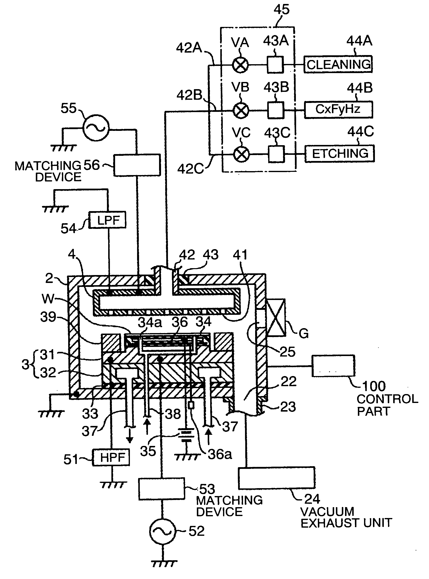
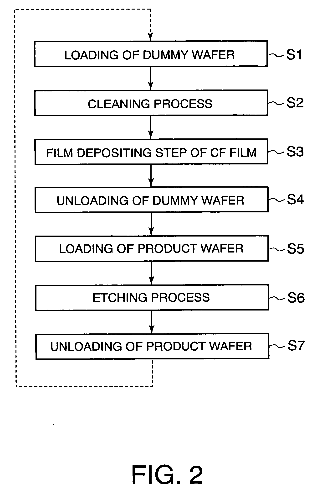
[0076]With the use of the plasma etching apparatus shown in FIG. 1, the cleaning process, the film depositing process of a CF film, and the etching process were performed in this order based on the steps S1 to S7 shown in FIG. 2. The etching process was performed to an SiN film formed on a wafer W. Regarding the cleaning process and the etching process, conditions common to the respective examples were employed. However, regarding the film depositing process of the CF film 21, a film depositing gas, a radiofrequency power, and a process period were varied as described below, while a process pressure of 26.6 Pa was unchanged.

[0077]With respect to each of the wafers W which had been etched in accordance with the above conditions, an average value of the etching rate, an in-plane uniformity of the etching rate, and the number of yttrium atoms on the wafer W were measured.

[0078]The average value of the etching rate was calculated from values measured at 33 measuring points located in th...


PUM

PropertyMeasurementUnit
frequencyaaaaaaaaaa
frequencyaaaaaaaaaa
pressureaaaaaaaaaa

Abstract

The present invention is a plasma etching method comprising: a cleaning step (a) in which a cleaning gas is supplied into a processing vessel and the cleaning gas is made plasma, so that a deposit adhering to an inside of the processing vessel is removed by means of the plasma; a film depositing step (b), succeeding the cleaning step (a), in which a film depositing gas containing carbon and fluorine is supplied into the processing vessel and the film depositing gas is made plasma, so that a film containing carbon and fluorine is deposited on the inside of the processing vessel by means of the plasma; an etching step (c), succeeding the film depositing step (b), in which a substrate is placed on a stage inside the processing vessel, and an etching gas is supplied into the processing vessel and the etching gas is made plasma, so that the substrate is etched by means of the plasma; and an unloading step (d), succeeding the etching step (c), in which the substrate is unloaded from the processing vessel; wherein, after the unloading step (d) has been finished, the cleaning step (a) to the unloading step (d) are repeated again.

Description

CROSS REFERENCE TO PRIOR APPLICATIONS[0001]This application claims priority from U.S. Provisional Application No. 61 / 071,367 filed on Apr. 24, 2008 and Japanese Patent Application No. 2008-027861 filed on Feb. 7, 2008. The entire contents of these applications are incorporated herein by reference.FIELD OF THE INVENTION[0002]The present invention relates to a technique for performing a plasma etching process to a substrate.BACKGROUND ART[0003]In a manufacturing method of a semiconductor substrate, such as a semiconductor wafer W (hereinafter referred to as “wafer”) and an FPD substrate, there is a step for subjecting the substrate to an etching process under a reduced-pressure atmosphere. An example of a plasma etching apparatus for performing this step is briefly described with reference to FIG. 13.[0004]In FIG. 13, the reference number 1 depicts a vacuum chamber. Disposed inside the vacuum chamber 1 is a stage 11 on which a substrate, e.g., a wafer W can be placed. There is dispose...

Claims


Application Information

Patent Timeline
Patent Type & Authority Applications(United States)
IPC IPC(8): H01L21/3065C23F1/08
CPCH01L21/3065B01D5/009B01D5/0051B01D5/0057B01D17/0208B01D2257/708
Inventor SAKAO, YOSUKEKAMIUTTANAI, KENSUKESHIMIZU, AKITAKA
Owner TOKYO ELECTRON LTD
Why Eureka
Try Eureka