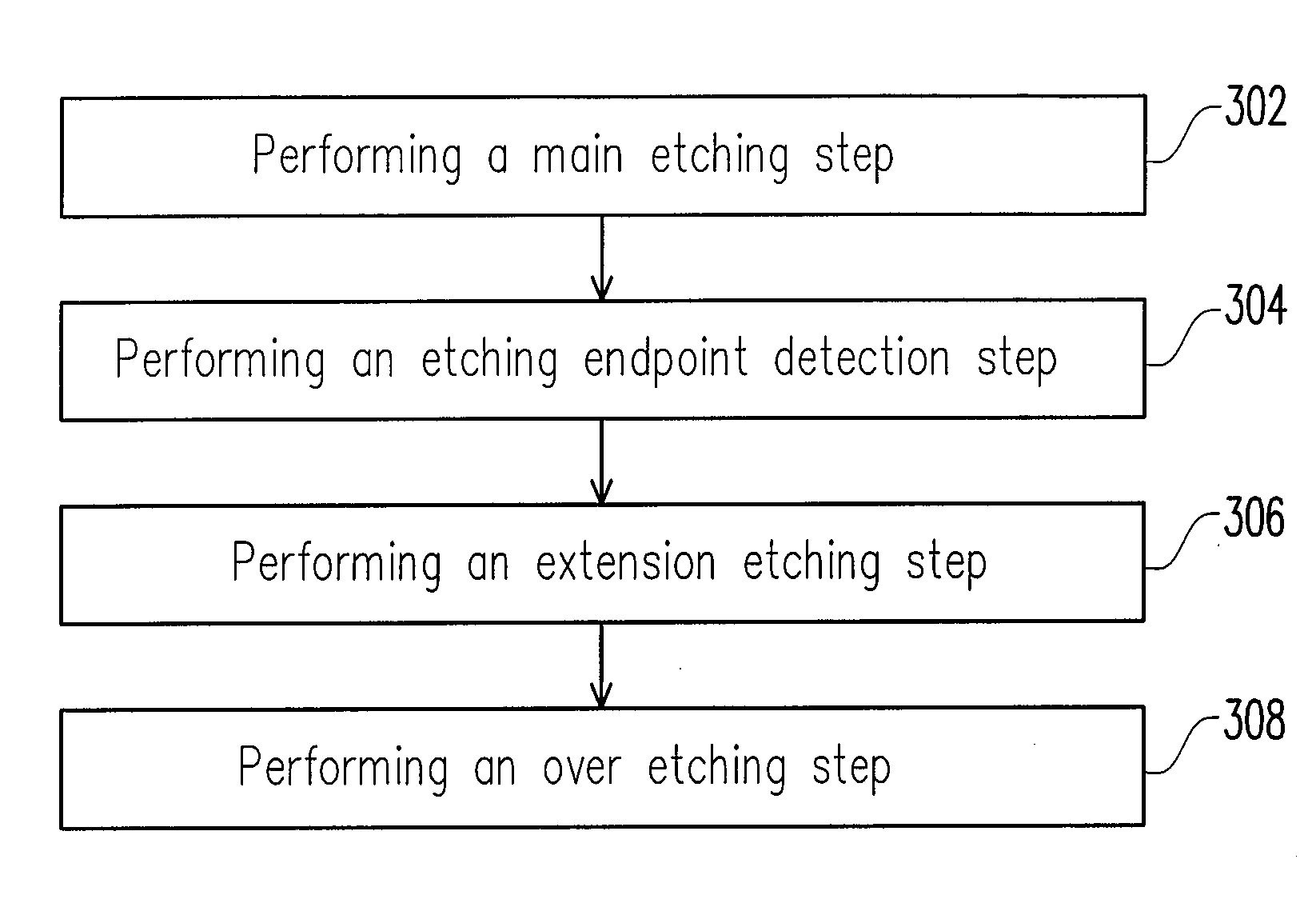
Patterning method

Active Publication Date: 2009-03-26
UNITED MICROELECTRONICS CORP
View PDF5 Cites 3 Cited by
  • Summary
  • Abstract
  • Description
  • Claims
  • Application Information

AI Technical Summary

Benefits of technology

[0007]The present invention is directed to a patterning method capable of effectively contro

Problems solved by technology

Variations in the CDs and the profiles may give rise to speed differences, and reliability of devices is correspondingly affected.
However, due to variations in manufacturing environment and in the manufacturing conditions, patterns formed by etching the polysilicon layer on within wafer or on without wafe

Method used


Image

  • Patterning method
  • Patterning method
  • Patterning method

Examples


Embodiment Construction

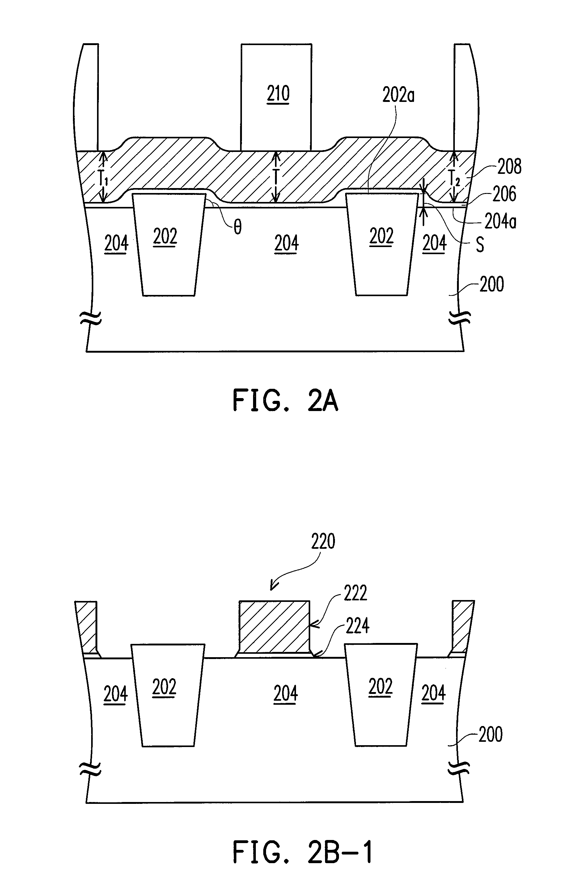
[0036]FIGS. 2A to 2B are schematic cross-sectional flowcharts illustrating the steps of manufacturing a gate structure according to an embodiment of the present invention.

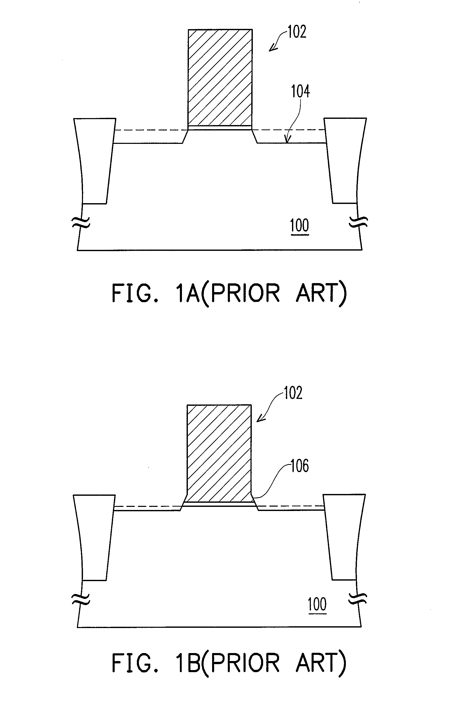
[0037]Referring to FIG. 2A, isolation structures 202 are formed in a substrate 200 to define active regions 204. The isolation structures 202 are STI structures, for example. After the isolation structures 202 are formed, a step height S of an upper surface of one of the isolation structures 202 and an upper surface of the substrate 200 or a side wall angle θ of the isolation structures 202 may be measured first. Then, a gate dielectric layer 206 is formed on the substrate 200. A material of the gate dielectric layer 206 is, for example, silicon oxide, silicon nitride, SiON or any material with a high dielectric constant, and the gate dielectric layer 206 may be formed through thermal oxidation or chemical vapor deposition (CVD), for example. Next, a gate conductive layer 208 is formed on the gate dielectric layer ...


PUM


Abstract

A patterning method is provided. In the patterning method, a film is formed on a substrate and a pre-layer information is measured. Next, an etching process is performed to etch the film. The etching process includes a main etching step, an etching endpoint detection step, an extension etching step and an over etching step. An extension etching time for performing the extension etching step is set within 10 seconds based on a predetermined correlation between an extension etching time and the pre-layer information, so as to achieve a required film profile.

Description

BACKGROUND OF THE INVENTION[0001]1. Field of the Invention[0002]The present invention relates to a method of manufacturing semiconductors, and more particularly, to a patterning method.[0003]2. Description of Related Art[0004]With development of semiconductor manufacturing technologies, critical dimensions (CDs) of features are minimized while integration of integrated circuits is continuously enhanced. In order to satisfy requirements for high density and great performance, it is necessary to precisely control the CDs of various features, profiles thereof, and uniformity thereof. In a complementary metal oxide semiconductor (CMOS) technology, a gate structure of a transistor is a key factor. Variations in the CDs and the profiles may give rise to speed differences, and reliability of devices is correspondingly affected. Accordingly, it is crucial to control a photolithography and etching process implemented for fabricating the gate structure.[0005]In a typical manufacturing process...

Claims


Application Information

Patent Timeline
IPC IPC(8): H01L21/66
CPCH01L22/26H01L21/76224
Inventor KUO, LUNG-ENLIAO, JIUNN-HSIUNGYANG, MIN-CHIEH
Owner UNITED MICROELECTRONICS CORP
Why Eureka
Try Eureka