
Antioxidants for post-cmp cleaning formulations

a technology of antioxidants and cleaning formulations, applied in the direction of lens cleaning compositions, detergent compositions, chemistry apparatus and processes, etc., can solve the problems of microelectronic device substrate residues, damage to copper lines, and severe roughening of copper metallization

Active Publication Date: 2009-09-24
ENTEGRIS INC
View PDF77 Cites 62 Cited by
  • Summary
  • Abstract
  • Description
  • Claims
  • Application Information

AI Technical Summary

Benefits of technology

[0024]continuously contacting the microelectronic device with the post-CMP residue-containing compo

Problems solved by technology

One particular issue in this respect is the residues that are left on the microelectronic device substrate following CMP processing.
If not removed, these residues can cause damage to copper lines or severely roughen the copper metallization, as well as cause poor adhesion of post-CMP applied layers on the device substrate.
Severe roughening of copper metallization is particularly problematic, since overly rough copper can cause poor electrical performance of the product microelectronic device.
Post-gas phase plasma etch residues, which may include chemical elements present on the substrate and in the plasma gases, are typically deposited on the back end of the line (BEOL) structures and if not removed, may interfere with subsequent silicidation or contact formation.
Conventional cleaning chemistries often damage the ILD, absorb into the pores of the ILD thereby increasing the dielectric constant, and / or corrode the metal structures.

Method used


Image

  • Antioxidants for post-cmp cleaning formulations
  • Antioxidants for post-cmp cleaning formulations
  • Antioxidants for post-cmp cleaning formulations

Examples


example 1

[0124]Blanketed PVD copper wafers were immersed in solutions including a basic solution comprising TMAH, 1-amino-2-propanol, and different antioxidants and the corrosion rate of copper determined using a potentiostat where the PVD Cu is the working electrode, Pt mesh is the counter electrode, and an Ag / AgCl electrode is the reference electrode. The copper anodic corrosion rates were calculated at anodic voltage biases from 0.1 to 1.0 V versus open circuit potentials. The results are summarized in Table 1 below.

CorrosionAntioxidantSolutionrate / Å min−1Control (TMAH + 1-12.28amino-2-propanol)15.03Ascorbic acid12 mL of 3500 ppm ascorbic acid in 200 g basic solution2.7218 mL of 3500 ppm ascorbic acid in 200 g basic solution2.6224 mL of 3500 ppm ascorbic acid in 200 g basic solution2.99uric acid22 mL of 3500 ppm uric acid in 300 g basic solution17.4722 mL of 3500 ppm uric acid in 300 g basic solution13.4325 mL of 35000 ppm uric acid in 300 g basic solution7.57Uric acid + oxalic25 mL of 35...

example 2

[0126]Compositions were employed for post-CMP cleaning of Sematech 854 pattern wafers having dried slurry and other PCMP residues on their surface. The wafer in each instance was cleaned on a Laurell Technologies Corporation (North Wales, Pa., USA) single wafer spin processor at 23° C. for 90 sec at 150 rpm using diluted removal concentrates A or D (concentrate D includes 5 wt. % TMAH; 9 wt. % 1-amino-2-propanol; 3.5 wt. % uric acid; 5 wt. % IPA; and 77.5 wt. % water), 30 sec at 150 rpm using deionized water, and 30 sec at 2500 rpm to spin dry the wafer. The cleaning compositions used were diluted 20 parts diluent (water) to 1 part removal concentrate prior to wafer processing.

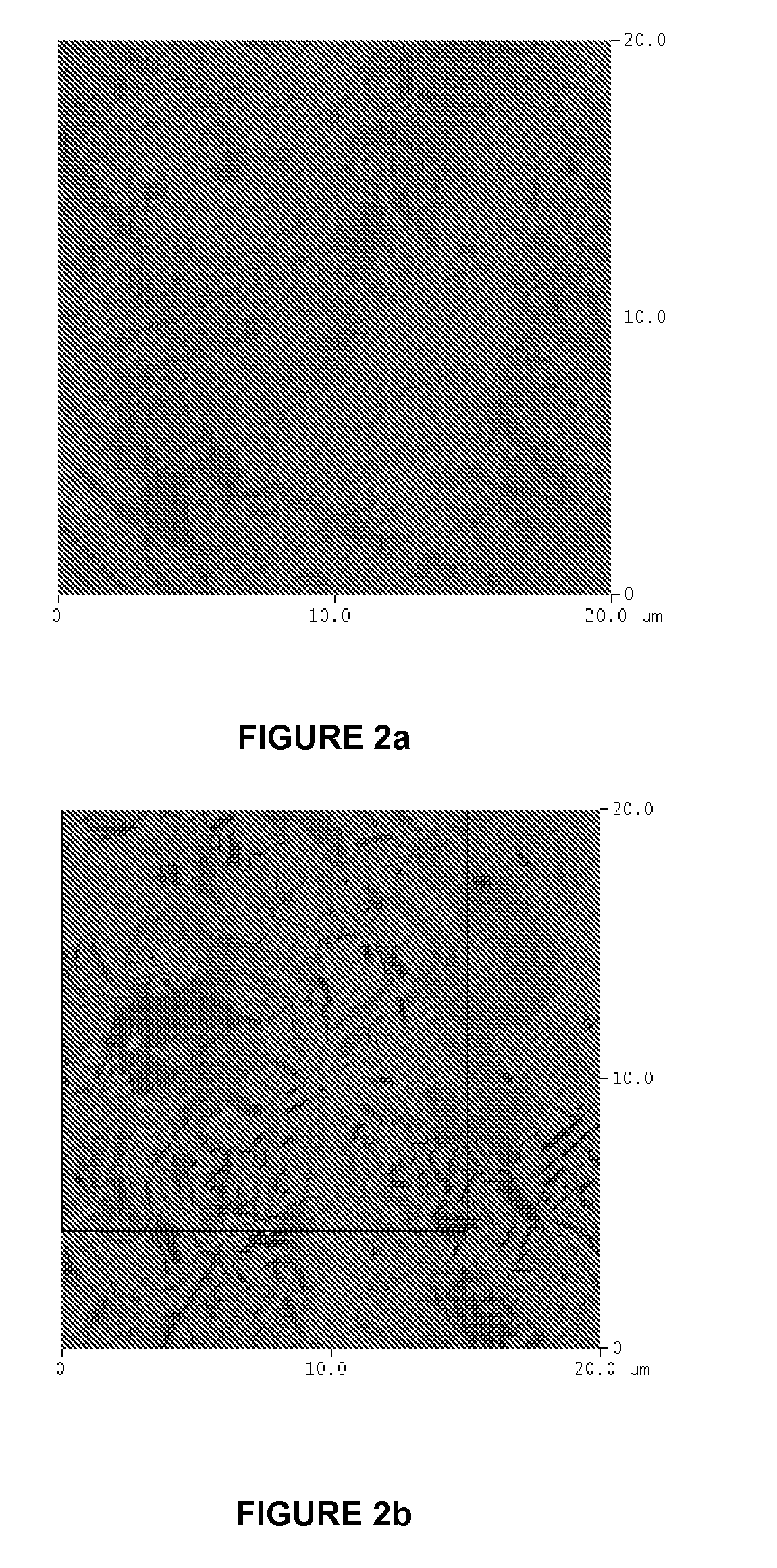
[0127]Following treatment, each wafer was subjected to atomic force microscopic (AFM) imaging (Digital Instruments Dimension 5000 Scanning Probe Microscope, Woodbury, N.Y., USA) to evaluate surface roughening. For each wafer sample, three random copper pads located towards the center of the wafer piece were se...


PUM


Abstract

An cleaning composition and process for cleaning post-chemical mechanical polishing (CMP) residue and contaminants from a microelectronic device having said residue and contaminants thereon. The cleaning compositions include novel corrosion inhibitors. The composition achieves highly efficacious cleaning of the post-CMP residue and contaminant material from the surface of the microelectronic device without compromising the low-k dielectric material or the copper interconnect material.

Description

CROSS-REFERENCE TO RELATED APPLICATIONS[0001]This application is a continuation-in-part of PCT Application No. PCT / U.S.07 / 79044, filed Sep. 20, 2007 in the name of David Angst et al., which claims priority to U.S. Provisional Patent Application No. 60 / 846,306, filed on Sep. 21, 2006 in the name of David Angst, and this application is also a continuation-in-part of PCT Application No. PCT / U.S.08 / 63885, filed May 16, 2008 in the name of Peng Zhang et al., which claims priority to U.S. Provisional Patent Application No. 60 / 938,591, filed on May 17, 2007 in the name of Peng Zhang et al., all of which are incorporated by reference in their respective entirety herein.FIELD[0002]The present invention relates generally to compositions including antioxidants for cleaning residue and / or contaminants from microelectronic devices having same thereon.DESCRIPTION OF THE RELATED ART[0003]Microelectronic device wafers are used to form integrated circuits. The microelectronic device wafer includes a...

Claims


Application Information

Patent Timeline
IPC IPC(8): C11D7/32
CPCC11D3/0084C11D3/0073C11D11/0047C11D7/32C11D7/265C11D7/267C11D7/3209C11D7/3281C11D2111/22C11D3/0078
Inventor ANGST, DAVIDZHANG, PENGBARNES, JEFFREYSONTHALIA, PRERNACOOPER, EMANUELBOGGS, KARL
Owner ENTEGRIS INC
Learn More