Junctions in substrate solar cells

a solar cell and substrate technology, applied in the direction of sustainable manufacturing/processing, final product manufacturing, vacuum evaporation coating, etc., can solve the problems of low efficiencies and instability high manufacturing cost of silicon solar cells,

Active Publication Date: 2009-10-01
FIRST SOLAR INC (US)
View PDF19 Cites 86 Cited by
  • Summary
  • Abstract
  • Description
  • Claims
  • Application Information

AI Technical Summary

Benefits of technology

[0011]In one embodiment there is disclosed a photovoltaic device having a substrate configuration comprising a transparent or opaque substrate, a metal electrode layer, a TCO layer an absorber layer comprising a Group II-VI semiconductor compound, a window layer, and an interface layer between the absorber layer and the window layer. Preferably the absorber layer comprises CdTe and the window layer comprises CdS. Further, the absorber layer and/or the interface layer comprise a thin film, nanoparticles and/or nanoparticles that are sintered. In one embodiment the absorber layer and/or the interface layer comprises a plurality of grain sizes. In one embodiment the interface layer comprises a Cd rich CdTe1-x where 0<x<1 composition. In another embodiment the interface layer comprises a Tellurium rich Cd1-xTe composition where 0<x<1. In one embodiment a portion of said interface layer located next to the absorber layer comprises large grains sizes, and a portion of said interface layer located next to the window layer comprises small grain sizes. In one embodiment the large grain sizes are about 2.0 μm to about 6.0 μm and the small grain sizes are about 0.1 μm to about 1.0 μm. In another embodiment the large grain sizes are about 2.0 μm to about 3.0 μm,

Problems solved by technology

Silicon solar cells are very expensive with manufacturing cost above $3.50/watt.
But by the end of that decade, and in the early 1990s, it was written off by many observers for its low efficiencies and instability.
The key obstacles to a-Si technology are low efficiencies, light-induced efficiency degradation (which requires more complicated cell designs such as multiple junctions), and process costs (fabrication methods are vacuum-based and fairly slow).
However, a-Si solar cells are expensive to manufacture (>$2.5/watt).
These record breaking small area devices have been fabricated using vacuum evaporation techniques which are capital intensive and quite costly.
However, it is very challenging to fabricate CIGS thin films of uniform composition on large area substrates.
This limitation also affects the process yield, which are generally quite low.
Because of these limitations, implementation of evaporation techniques has not been successful for large-scale, low-cost commercial production of CIGS solar cells.

Method used


Image

  • Junctions in substrate solar cells
  • Junctions in substrate solar cells
  • Junctions in substrate solar cells

Examples


Embodiment Construction

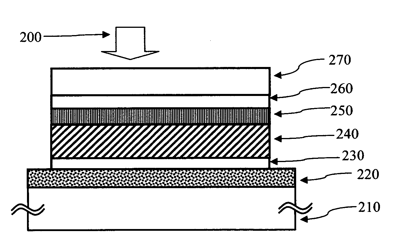
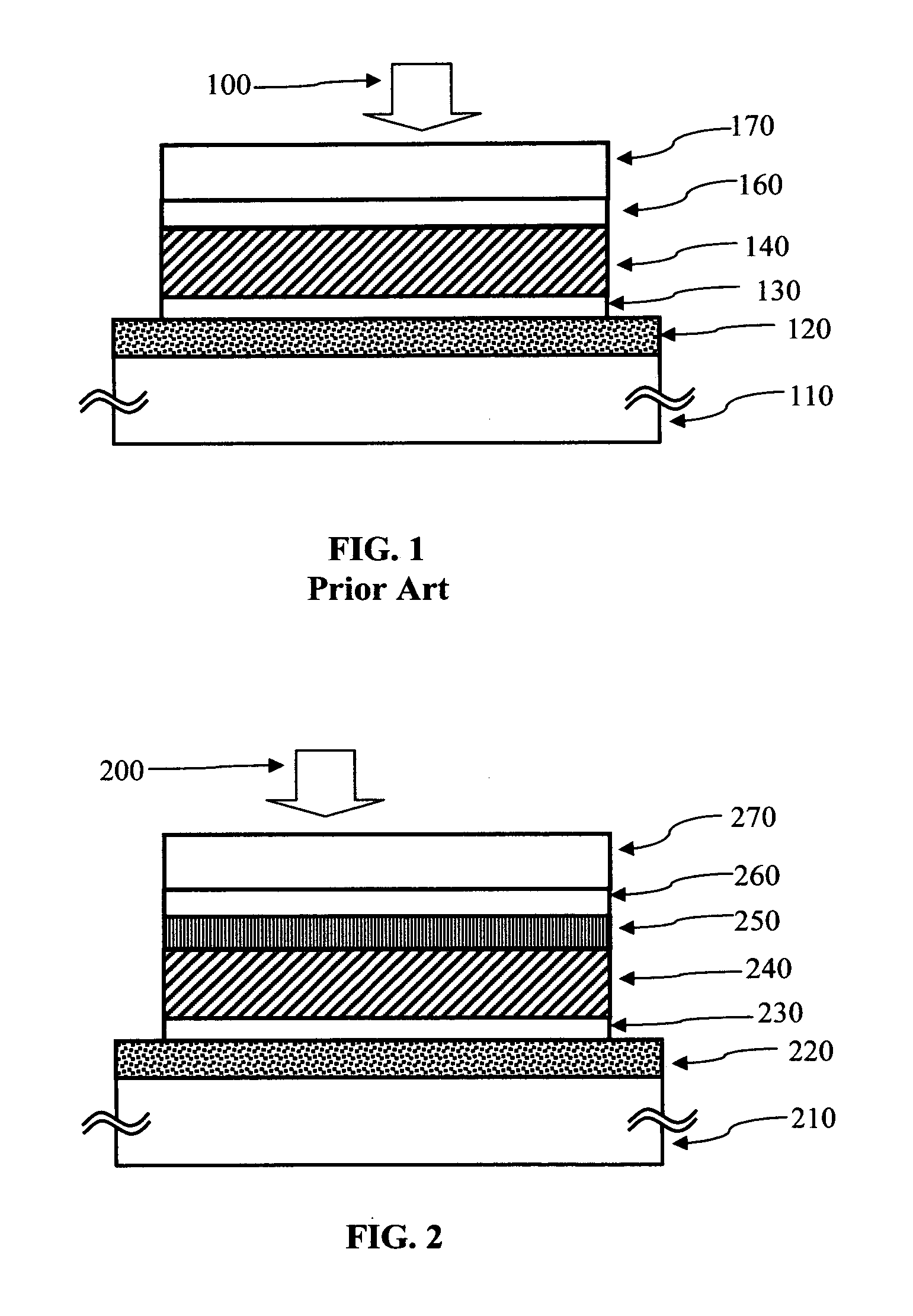
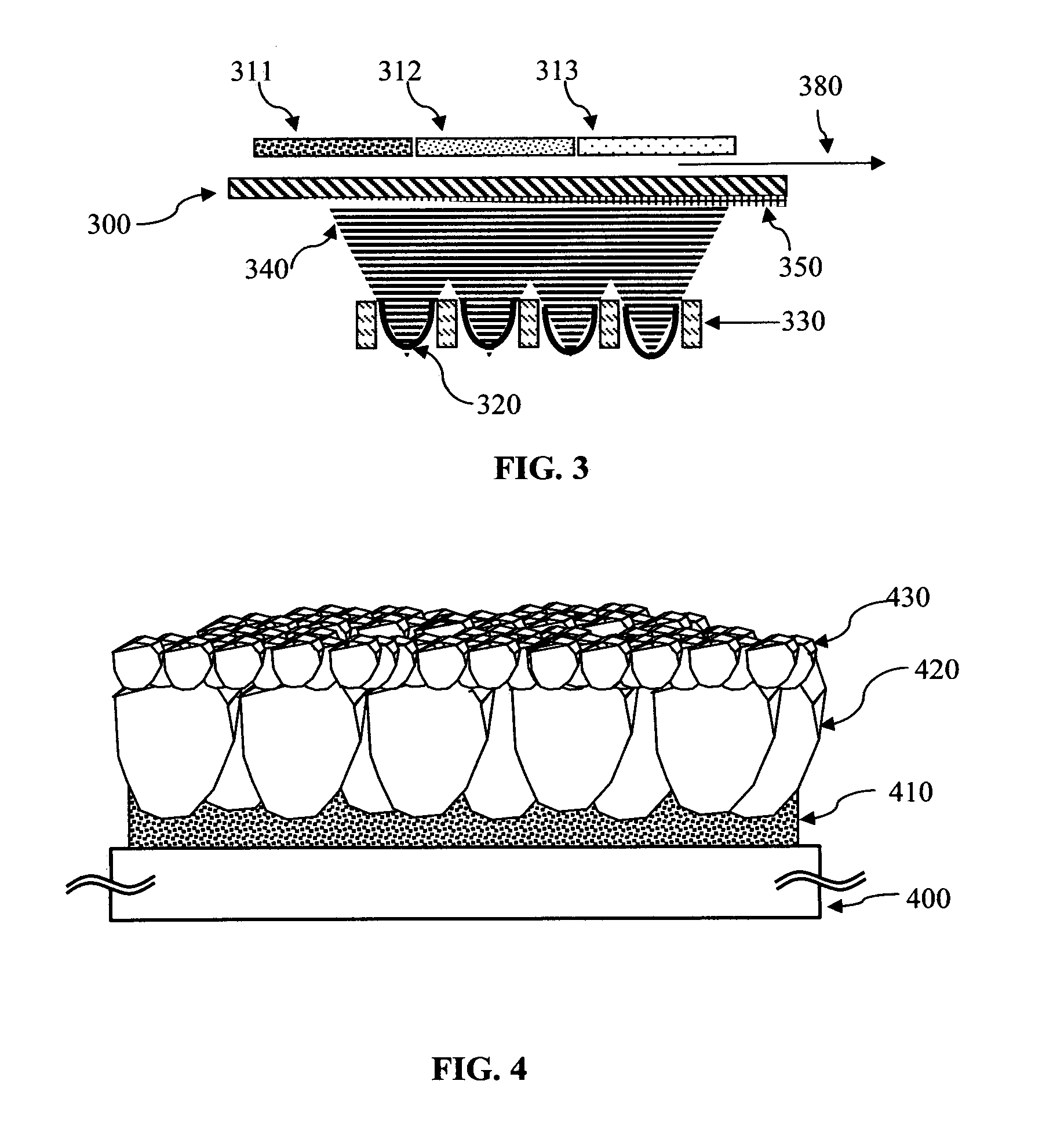
[0019]Reference will now be made in detail to some specific embodiments of the invention including the best modes contemplated by the inventors for carrying out the invention. Examples of these specific embodiments are illustrated in the accompanying drawings. While the invention is described in conjunction with these specific embodiments, it will be understood that it is not intended to limit the invention to the described embodiments. On the contrary, it is intended to cover alternatives, modifications, and equivalents as may be included within the spirit and scope of the invention as defined by the appended claims. In the following description, numerous specific details are set forth in order to provide a thorough understanding of the present invention. The present invention may be practiced without some or all of these specific details. In this specification and the appended claims, the singular forms “a,”“an,” and “the” include plural reference unless the context clearly dictat...


PUM

PropertyMeasurementUnit
Timeaaaaaaaaaa
Lengthaaaaaaaaaa
Lengthaaaaaaaaaa

Abstract

The present invention discloses thin film photovoltaic devices comprising Group II-VI semiconductor layers with a substrate configuration having an interface layer between the absorber layer and the window layer to create improved junctions.
The present invention also discloses methods for making and surface treatments for thin film photovoltaic devices comprising Group II-VI semiconductor layers with a substrate configuration to create devices with improved junctions.

Description

CROSS REFERENCE TO RELATED APPLICATIONS[0001]This application claims priority to U.S. Provisional Patent Application Ser. No. 61 / 070,903 filed Mar. 26, 2008 the contents of which is incorporated herein by reference.BACKGROUND OF THE INVENTION[0002]Increasing oil prices have heightened the importance of developing cost effective renewable energy. Significant efforts are underway around the world to develop cost effective solar cells to harvest solar energy. In order for solar cells to be cost effective with traditional sources of energy solar cells must be manufactured at a cost well below $1 / watt.[0003]Current solar energy technologies can be broadly categorized as crystalline silicon and thin film technologies. Approximately 90% of the solar cells are made from silicon—single crystal silicon or polycrystalline silicon. Crystalline silicon (c-Si) has been used as the light-absorbing semiconductor in most solar cells, even though it is a relatively poor absorber of light and requires...

Claims


Application Information

Patent Timeline
IPC IPC(8): H01L31/0256H01L31/18
CPCC23C14/0629C23C14/24C23C14/54Y02E10/543H01L31/073H01L31/1836C23C14/562Y02P70/50
Inventor PAULSON, PUTHURHOTZ, CHARLIELEIDHOLM, CRAIGREDDY, DAMODER
Owner FIRST SOLAR INC (US)
Why Eureka
Try Eureka