Method of Creating Alignment/Centering Guides for Small Diameter, High Density Through-Wafer Via Die Stacking

a technology of through-wafer and guide, which is applied in the direction of semiconductor/solid-state device details, semiconductor devices, line/current collector details, etc., can solve the problems of die alignment during manufacturing and may present challenges

Active Publication Date: 2009-10-15
MICRON TECH INC
View PDF15 Cites 76 Cited by
  • Summary
  • Abstract
  • Description
  • Claims
  • Application Information

AI Technical Summary

Problems solved by technology

However, because the TSVs must align throughout the stacked dies of the circuit, alignment of the dies during manufacturing may present challenges, especially with respect to small diameter and / or higher density TSVs.

Method used


Image

  • Method of Creating Alignment/Centering Guides for Small Diameter, High Density Through-Wafer Via Die Stacking
  • Method of Creating Alignment/Centering Guides for Small Diameter, High Density Through-Wafer Via Die Stacking
  • Method of Creating Alignment/Centering Guides for Small Diameter, High Density Through-Wafer Via Die Stacking

Examples


Embodiment Construction

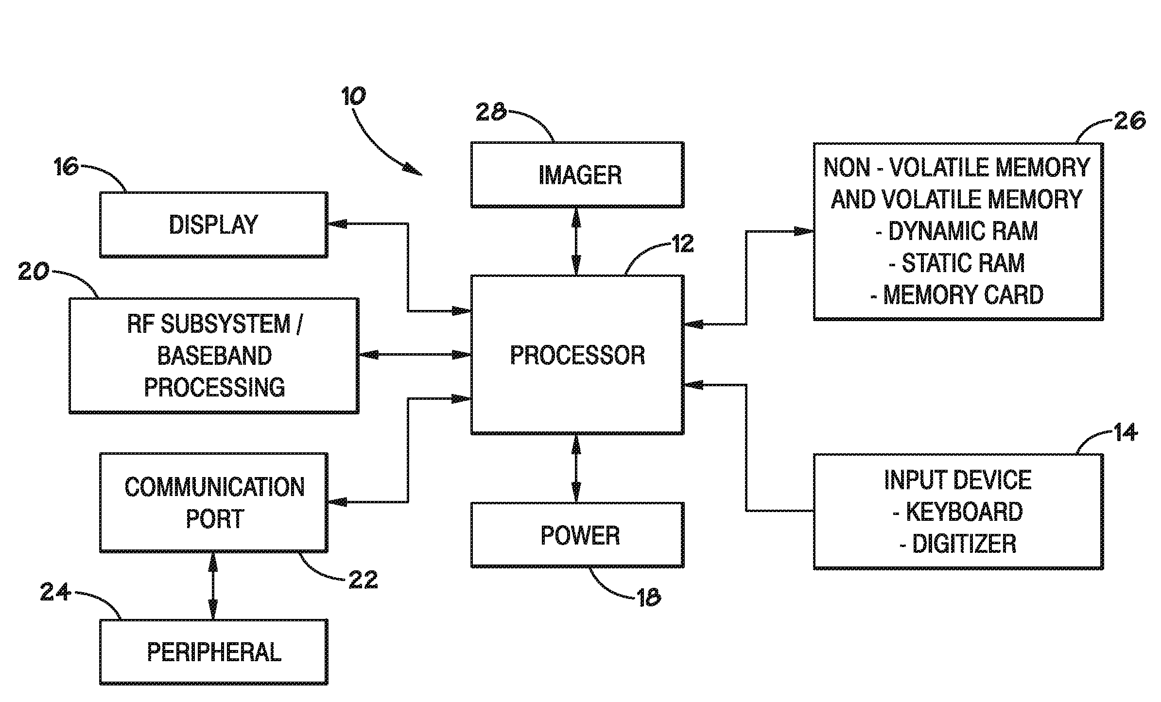
[0015]FIG. 1 is a block diagram of an electronic system containing integrated circuit devices that may employ embodiments of the present invention. The electronic device or system, which is generally indicated by the reference numeral 10, may be any of a variety of types, such as a computer, digital camera, cellular phone, personal organizer, or the like. In a typical processor-based device, a processor 12, such as a microprocessor, controls the operation of system functions and requests.

[0016]Various devices may be coupled to the processor 12 depending on the functions that the system 10 performs. For example, an input device 14 may be coupled to the processor 12 to receive input from a user. The input device 14 may comprise a user interface and may include buttons, switches, a keyboard, a light pen, a mouse, a digitizer, a voice recognition system, or any of a number of other input devices. An audio or video display 16 may also be coupled to the processor 12 to provide information...


PUM

PropertyMeasurementUnit
densityaaaaaaaaaa
electrical connectivityaaaaaaaaaa
lengthaaaaaaaaaa

Abstract

A method if provided for forming a die stack. The method includes forming a plurality of through-wafer vias and a first plurality of alignment features in a first die. A second plurality of alignment features is formed in a second die, and the first die is stacked on the second die such that the first plurality of alignment features engage the second plurality of alignment features. A method of manufacturing a die stack is also provided that includes forming a plurality of through-wafer vias on a first die, forming a plurality of recesses on a first die, and forming a plurality of protrusions on a second die. A die stack and a system are also provided.

Description

BACKGROUND OF THE INVENTION[0001]1. Field of the Invention[0002]The present invention relates generally to semiconductor devices and, more particularly, to stackable dies using through-wafer vias.[0003]2. Description of the Related Art[0004]Microprocessor-controlled circuits are used in a wide variety of applications. Such applications include personal computers, cellular phones, digital cameras, control systems, and a host of other consumer products. A personal computer, digital camera, or the like, generally includes various components, such as microprocessors, that handle different functions for the system. By combining these components, various consumer products and systems may be designed to meet specific needs. Microprocessors are essentially generic devices that perform specific functions under the control of software programs. These software programs are generally stored in one or more memory devices that are coupled to the microprocessor and / or other peripherals.[0005]Elect...

Claims


Application Information

Patent Timeline
Patent Type & Authority Applications(United States)
IPC IPC(8): H02G3/00H01R43/00
CPCH01L23/481Y10T29/49117H01L24/81H01L25/0657H01L25/50H01L2224/13009H01L2224/13099H01L2224/13147H01L2224/81136H01L2224/81801H01L2225/06513H01L2225/06541H01L2924/01029H01L2924/01033H01L2924/01046H01L2924/01049H01L2924/01074H01L2924/01078H01L2924/01079H01L2924/14H01L2924/01047H01L2924/0105H01L2924/01075H01L2924/014H01L2224/10135H01L2224/10165H01L2224/81139H01L2224/8114H01L2224/81141H01L2224/8014H01L24/12
Inventor PRATT, DAVE
Owner MICRON TECH INC
Why Eureka
Try Eureka