Two bit u-shaped memory structure and method of making the same

a memory structure and two-bit technology, applied in the field of memory structure, can solve the problems of process control problems, shrinkage of flash memory cells, etc., and achieve the effects of increasing the gate induced leakage effect, improving control problems, and increasing the performance of flash memory

Active Publication Date: 2009-10-15
NAN YA TECH
View PDF8 Cites 1 Cited by
  • Summary
  • Abstract
  • Description
  • Claims
  • Application Information

AI Technical Summary

Benefits of technology

[0008]A novel memory structure and a fabricating method are provided in the present invention. According to the invention, the floating gates of the flash memory have U-shaped bottoms. In this way, not only can the floating gate channel be extended even though the size of the device is scaled down but the performance of the flash memory can also be increased. A local doping region is positioned below the floating gates directly in order to replace the conventional pocket doping region. Therefore, the control problem can be improved. In addition, the memory structure provided in the invention can increase the gate induced leakage (GIDL) effect. In this way, the programming and reading speed of the flash memory is increased.

Problems solved by technology

As electronic devices become smaller, the size of the flash memory cells is also shrinking.
Because the pocket doping region is adjacent to the source / drain doping region, during the fabricating process the pocket doping region will be influenced by the source / drain doping region, leading to problems in process control.

Method used


Image

  • Two bit u-shaped memory structure and method of making the same
  • Two bit u-shaped memory structure and method of making the same
  • Two bit u-shaped memory structure and method of making the same

Examples


Embodiment Construction

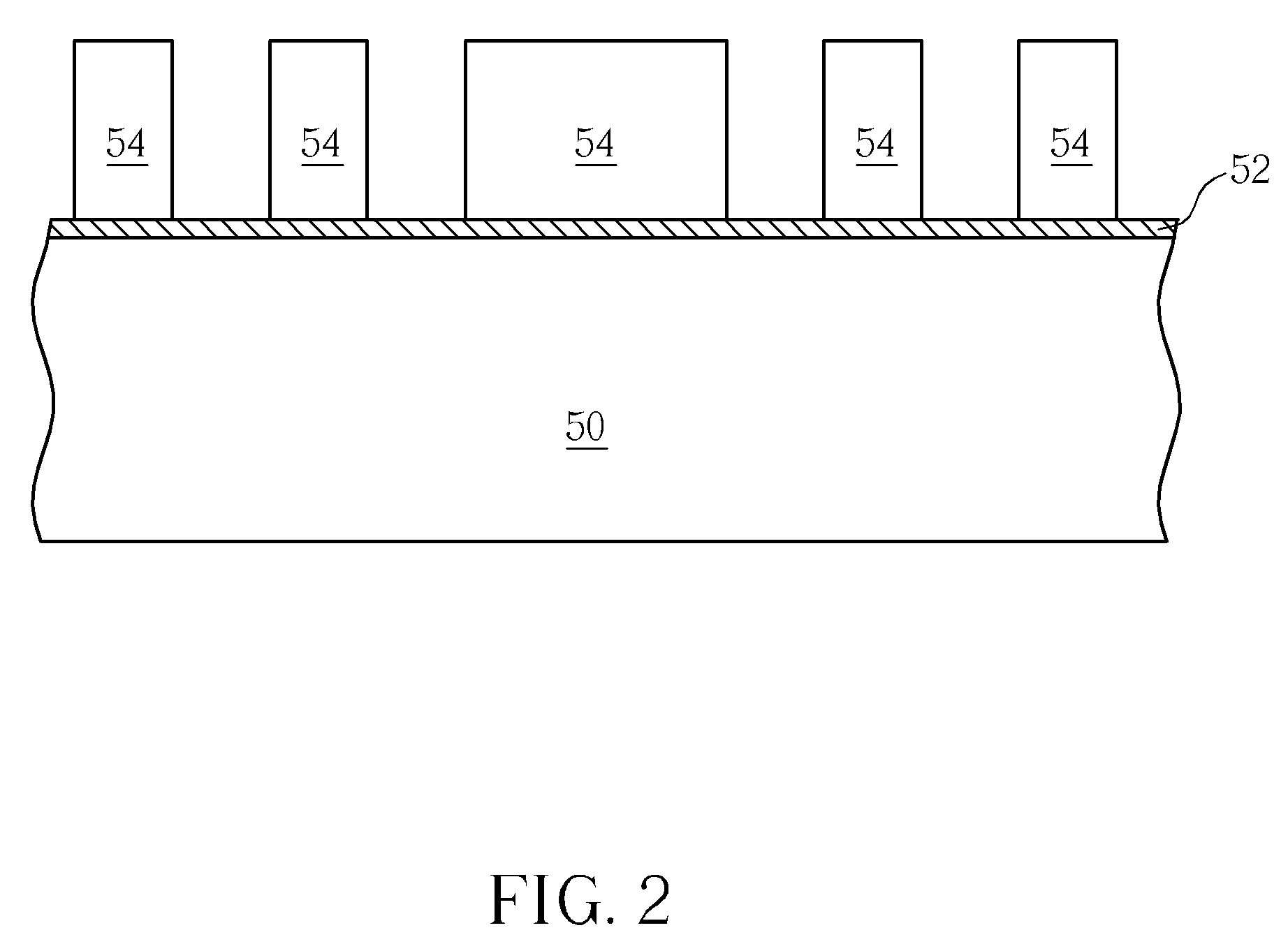
[0014]FIG. 2 to FIG. 7 are schematic diagrams depicting the fabricating method for the memory structure of the present invention. As shown in FIG. 2, a substrate 50 is provided. The substrate 50 is covered by a dielectric layer 52 and a patterned hard mask layer 54. The dielectric layer 52 includes silicon oxide and the hard mask layer 54 includes silicon nitride 54.

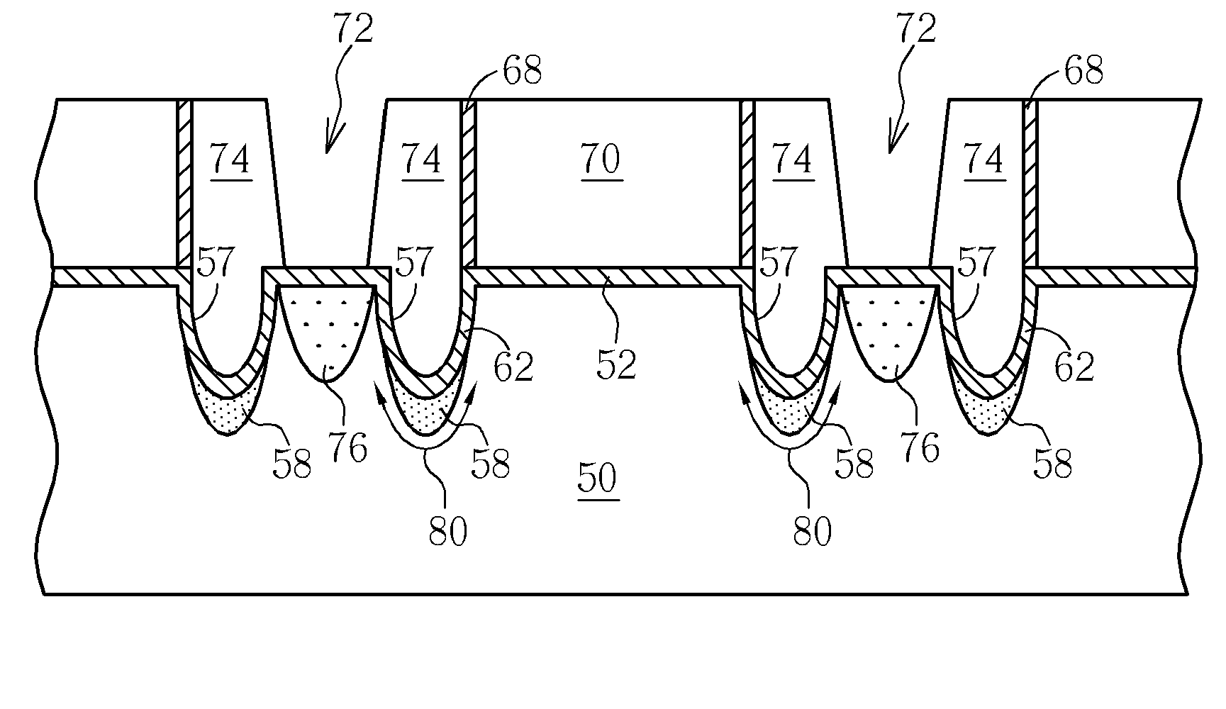
[0015]As shown in FIG. 3, a trench 56 is formed in the substrate 50 by taking the hard mask layer 54 as a mask. The trench 56 has a U-shaped bottom 57. Then, a local doping region 58 is formed in the substrate 50 around the U-shaped bottom 57 of the trench 56. Next, the hard mask layer 54 and the dielectric layer 52 in the region 60 are removed by utilizing a photo mask (not shown), and the substrate 50 in region 60 is thereby exposed.

[0016]As shown in FIG. 4, a dielectric layer 62 acting as a tunnel oxide layer is formed on the surface of the trench 56 and on the surface of the substrate 50 in the region 60. According t...


PUM


Abstract

A memory structure includes: a substrate; a control gate positioned on the substrate; floating gates positioned at two sides of the control gate, wherein the floating gates have a U-shaped bottom embedded in the substrate; a first dielectric layer positioned between the control gate and the substrate; a second dielectric layer positioned between the U-shaped bottom of the floating gates and the substrate; a third dielectric layer positioned between the control gate and the floating gates; a local doping region positioned around the floating gates channel; and a source/drain doping region positioned in the substrate at a side of the floating gates.

Description

BACKGROUND OF THE INVENTION[0001]1. Field of the Invention[0002]The present invention relates to a memory structure and method of fabricating the memory structure, and more particularly, to a two bit memory structure having floating gates with a U-shaped bottom and a method of making the two bit memory structure.[0003]2. Description of the Prior Art[0004]A flash memory is a memory device that allows multiple data writing, reading, and erasing operations. It is a technology that is used widely, and primarily used for portable products. As electronic devices become smaller, the size of the flash memory cells is also shrinking. Currently, scaling down of flash memory cells is considered critical in continuing the trend toward higher device density.[0005]FIG. 1 shows a structure of a two-bit flash memory cell according to the prior art. As shown in FIG. 1, the structure of the conventional two-bit flash memory cell comprises: a substrate 10, a control gate 12 positioned on the substrate...

Claims


Application Information

Patent Timeline
Patent Type & Authority Applications(United States)
IPC IPC(8): H01L29/788H01L21/336
CPCH01L27/115H01L27/11521H01L29/1037H01L29/7887H01L29/42336H01L29/66825H01L29/1041H10B69/00H10B41/30
Inventor LIAO, WEI-MINGWANG, JER-CHYI
Owner NAN YA TECH
Why Eureka
Try Eureka