Metal gate compatible flash memory gate stack

Active Publication Date: 2009-10-15
GLOBALFOUNDRIES US INC
View PDF11 Cites 72 Cited by
  • Summary
  • Abstract
  • Description
  • Claims
  • Application Information

AI Technical Summary

Benefits of technology

[0010]The present invention addresses the needs described above by providing a first gate stack comprising two gate electrodes and configured for a flash memory device, a sec

Problems solved by technology

Oftentimes, providing both such enhancement in performance and multiple device types in the same semiconductor chip increases processing costs.
Typically, high gate leakage current of silicon oxide and nitrided silicon dioxide as well as depletion effect o

Method used


Image

  • Metal gate compatible flash memory gate stack
  • Metal gate compatible flash memory gate stack
  • Metal gate compatible flash memory gate stack

Examples


first embodiment

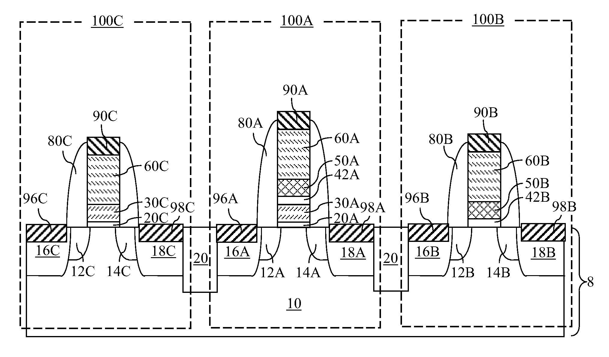
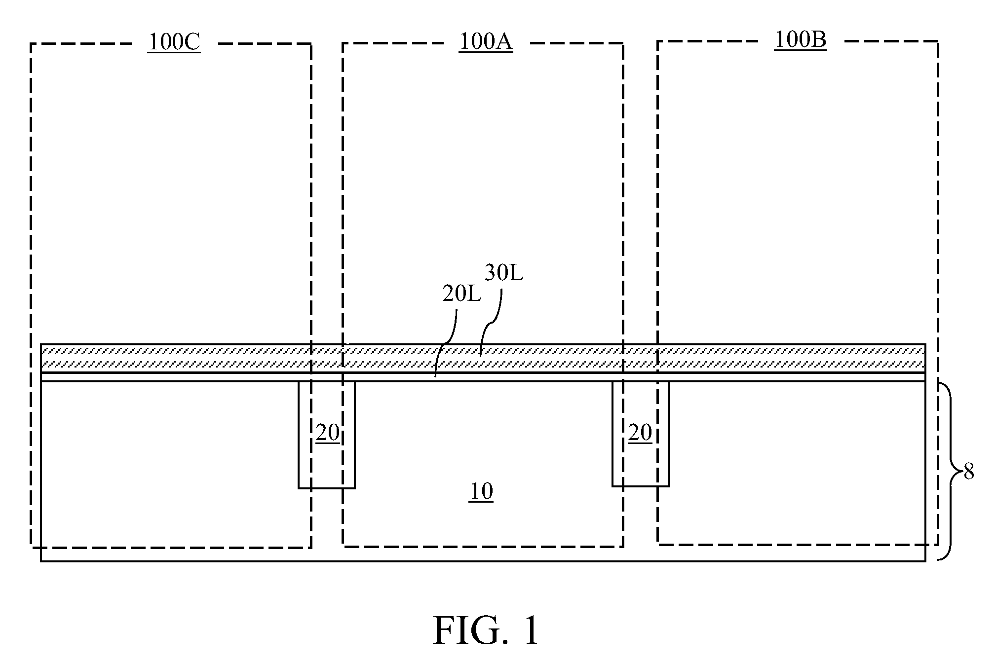
[0064]Referring to FIG. 1, a first exemplary semiconductor structure according to the present invention comprises a semiconductor substrate 8 containing a substrate semiconductor layer 10 comprising a semiconductor material, which may be selected from, but is not limited to, silicon, germanium, silicon-germanium alloy, silicon carbon alloy, silicon-germanium-carbon alloy, gallium arsenide, indium arsenide, indium phosphide, III-V compound semiconductor materials, II-VI compound semiconductor materials, organic semiconductor materials, and other compound semiconductor materials. Preferably, the substrate semiconductor layer 10 is single crystalline, i.e., have the same set of crystallographic orientations, or “epitaxial.”

[0065]The semiconductor substrate 8 may be a bulk substrate, a semiconductor-on-insulator (SOI) substrate, or a hybrid substrate having a bulk portion and an SOI portion. While the first embodiment is described with a bulk substrate, embodiments employing an SOI subs...

second embodiment

[0105]Referring to FIG. 15, a second exemplary semiconductor structure according to the present invention is derived from the first exemplary semiconductor structure by omitting the formation of the interfacial dielectric layer 40L in the first exemplary semiconductor structure. At a processing step corresponding to FIG. 3, the high-k gate dielectric layer 42L is formed directly on the top surface of the first doped semiconductor layer 30L and the exposed surface of the substrate semiconductor layer 10 in the second device region 100B. Thus, the first gate stack in the first device region 100A comprises, from bottom to top, the first semiconductor oxide containing gate dielectric portion 20A, the first doped semiconductor first-region portion 30A, the first high-k gate dielectric portion 42A, the first metal gate portion 50A, the first optional semiconductor material portion 52A, and the second doped semiconductor first-region portion 60A. The second gate stack comprises, from botto...

third embodiment

[0106]Referring to FIG. 16, a third exemplary semiconductor structure according to the present invention is derived from the first exemplary semiconductor structure by omitting the formation of the optional semiconductor material layer 52L in the first exemplary semiconductor structure. At a processing step corresponding to FIG. 7, the second doped semiconductor layer 60L is formed directly on the top surface of the metal gate layer 50L and the exposed top surface of the first doped semiconductor layer 30L in the third device region 100C. Thus, the first gate stack in the first device region 100A comprises, from bottom to top, the first semiconductor oxide containing gate dielectric portion 20A, the first doped semiconductor first-region portion 30A, the fist interfacial dielectric portion 40A, the first high-k gate dielectric portion 42A, the first metal gate portion 50A, and the second doped semiconductor first-region portion 60A. The second gate stack comprises, from bottom to to...


PUM


Abstract

A first gate stack comprising two stacked gate electrodes in a first device region, a second gate stack comprising a metal gate electrode in a second device region, and a third gate stack comprising a semiconductor gate electrode in a third device region are formed by forming and removing portions of a silicon-oxide based gate dielectric layer, a first doped semiconductor layer, an interfacial dielectric layer, a high-k gate dielectric layer, a metal gate layer, and an optional semiconductor material layer in various device regions. The first gate stack may be employed to form a flash memory, and the second and third gate stacks may be employed to form a pair of p-type and n-type field effect transistors.

Description

FIELD OF THE INVENTION[0001]The present invention generally relates to semiconductor devices, and particularly to semiconductor structures including a flash memory gate stack, a metal gate structure, and a semiconductor gate structure, and methods of manufacturing the same.BACKGROUND OF THE INVENTION[0002]Advanced semiconductor chips require enhancement in performance through device performance as well as expanded offering in device types to enable multiple types of devices providing useful functionality. Oftentimes, providing both such enhancement in performance and multiple device types in the same semiconductor chip increases processing costs. Thus, providing as many device types as possible, while limiting processing complexity within reasonable limits, helps provide a highly functional semiconductor chip at a reasonable processing cost.[0003]On one hand, a key performance parameter of advanced semiconductor chips is on-current and off-current of field effect transistors. Typica...

Claims


Application Information

Patent Timeline
IPC IPC(8): H01L29/00H01L21/3205
CPCH01L21/823842H01L27/11543H01L27/11526H01L21/823857H10B41/40H10B41/48
Inventor BOOTH, JR., ROGER A.KIM, DEOK-KEEYANG, HAINING S.YU, XIAOJUN
Owner GLOBALFOUNDRIES US INC
Why Eureka
Try Eureka