

Microwave introduction device
a technology of introduction device and microwave, which is applied in the field of microwave introduction device, can solve the problems of microwave to have an unnecessary oscillation mode or reflectivity, microwave leakage or adverse influence on microwave radiation,
- Summary
- Abstract
- Description
- Claims
- Application Information
AI Technical Summary
Benefits of technology
Problems solved by technology
Method used
Image

Examples
Embodiment Construction
[0039]Hereinafter, a microwave introduction device and a plasma processing apparatus in accordance with an embodiment of the present invention will be described in detail with reference to the accompanying drawings.
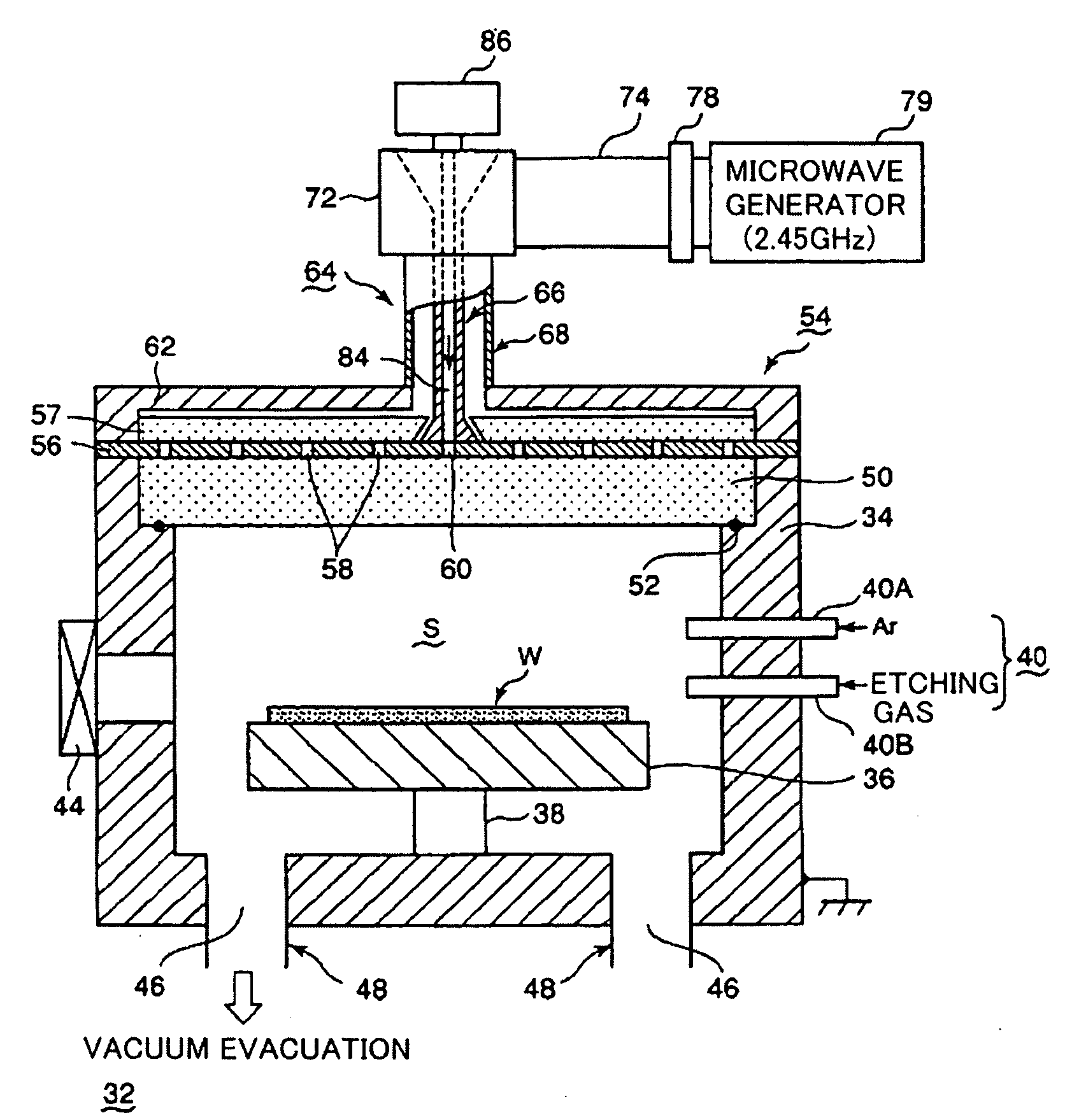
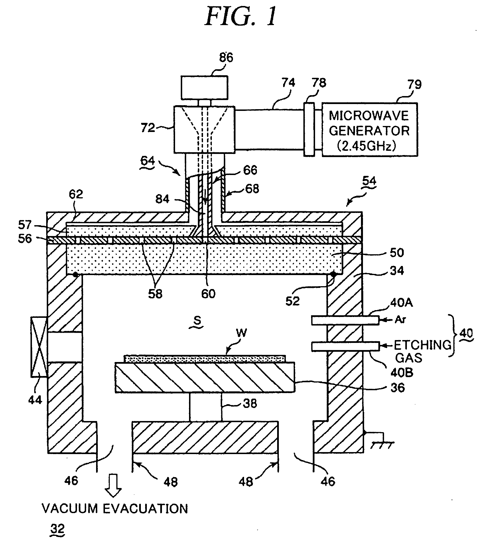
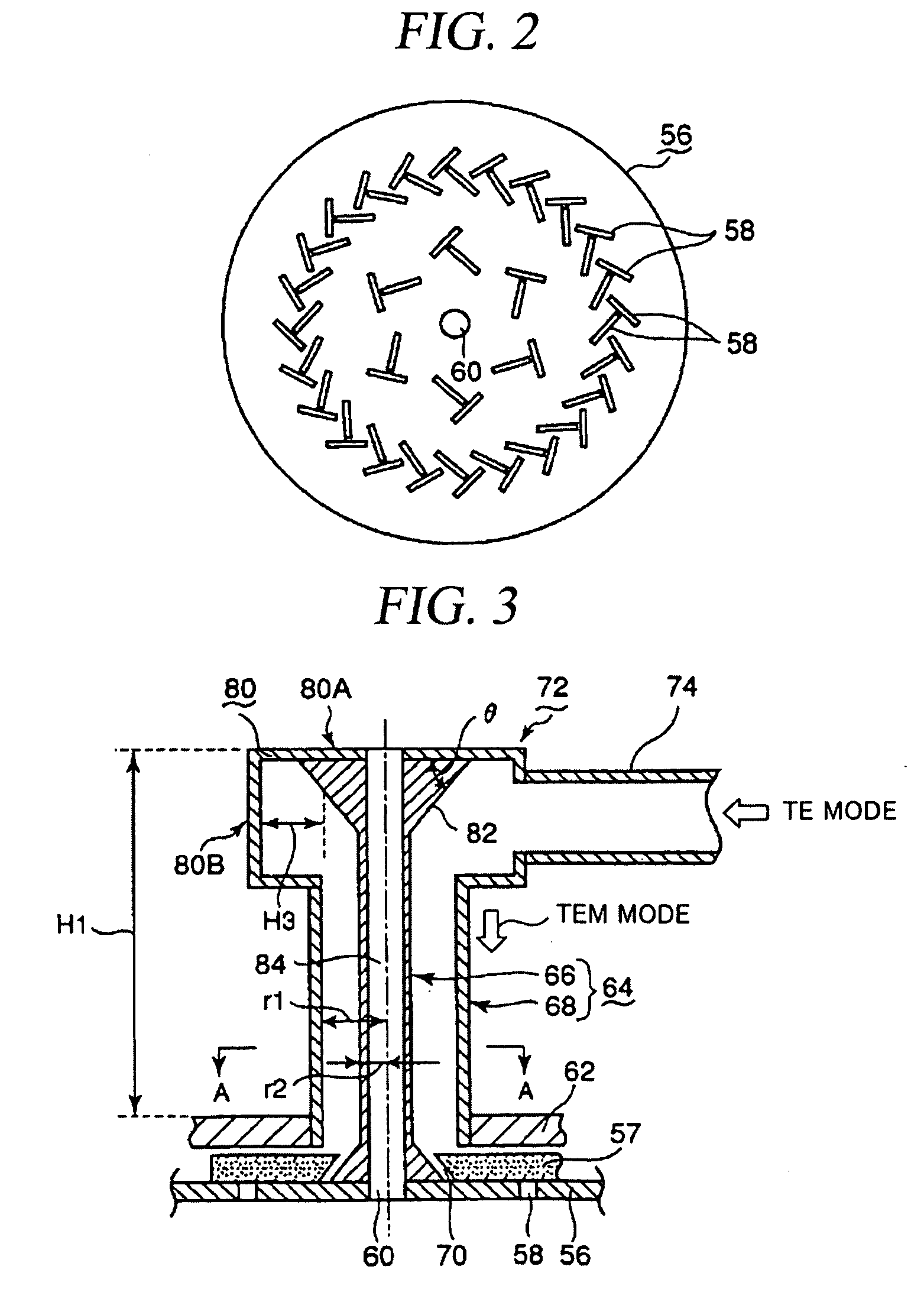
[0040]FIG. 1 provides a configuration view of a plasma processing apparatus in accordance with an embodiment of the present invention. FIG. 2 presents a plan view of a planar antenna member of the plasma processing apparatus described in FIG. 1. FIG. 3 illustrates an enlarged cross-sectional view of a microwave introduction device of the plasma processing apparatus depicted in FIG. 1. FIG. 4 shows a cross-sectional view taken along the line A-A in FIG. 3. FIG. 5 depicts a plan view of a mode converter of the plasma processing apparatus illustrated in FIG. 1. Herein, an etching process will be described as an example of a plasma process.
[0041]As shown in FIG. 1, a plasma processing apparatus (plasma etching apparatus) 32 in accordance with the embodiment of the present inv...
PUM
| Property | Measurement | Unit |
|---|---|---|
| impedance | aaaaa | aaaaa |
| inner diameter D1 | aaaaa | aaaaa |
| frequency | aaaaa | aaaaa |
Abstract
Description
Claims
Application Information