Laser processing method for transparent plate

a technology of transparent plate and laser processing method, which is applied in glass making apparatus, manufacturing tools, instruments, etc., can solve the problems of reducing yield, glass substrate may not be reliably broken along the breaking line, and the method is not always satisfactory

Inactive Publication Date: 2009-10-29
DISCO CORP
View PDF4 Cites 2 Cited by
  • Summary
  • Abstract
  • Description
  • Claims
  • Application Information

AI Technical Summary

Benefits of technology

[0009]It is therefore an object of the present invention to provide a laser processing method for a transparent plate such as a glass plate which can form a laser processed groove on the transparent plate without the generation of cracks.
[0013]According to the present invention, the pulsed laser beam to be applied to the transparent plate has an absorption wavelength to the transparent plate. Further, the repetition frequency of the pulsed laser beam is 200 kHz or more and the energy density per pulse of the pulsed laser beam is 3.8 J / cm2 or more. Accordingly, the laser processed groove can be formed on the transparent plate without the generation of cracks in the transparent plate.

Problems solved by technology

In this method of breaking the glass substrate by forming the scribe line along the breaking line on the outer surface of the glass substrate and next applying an external force along this scribe line, there is a possibility that the glass substrate may not be reliably broken along the breaking line, causing a reduction in yield.
Accordingly, this method is not always satisfactory from the viewpoint of productivity.
However, according to the experiment conducted by the present inventors, it has been found that the pulsed laser beam may pass through the glass substrate to damage the electrodes formed on the inner surface of the silicon substrate.
Further, according to the experiment conducted by the present inventors, it has also been found that when the repetition frequency of the pulsed laser beam applied to the glass substrate is low, the application period of pulses is long, so that a cooling time becomes long and a tensile stress due to cooling is generated to cause cracks in the glass substrate.

Method used


Image

  • Laser processing method for transparent plate
  • Laser processing method for transparent plate
  • Laser processing method for transparent plate

Examples


Embodiment Construction

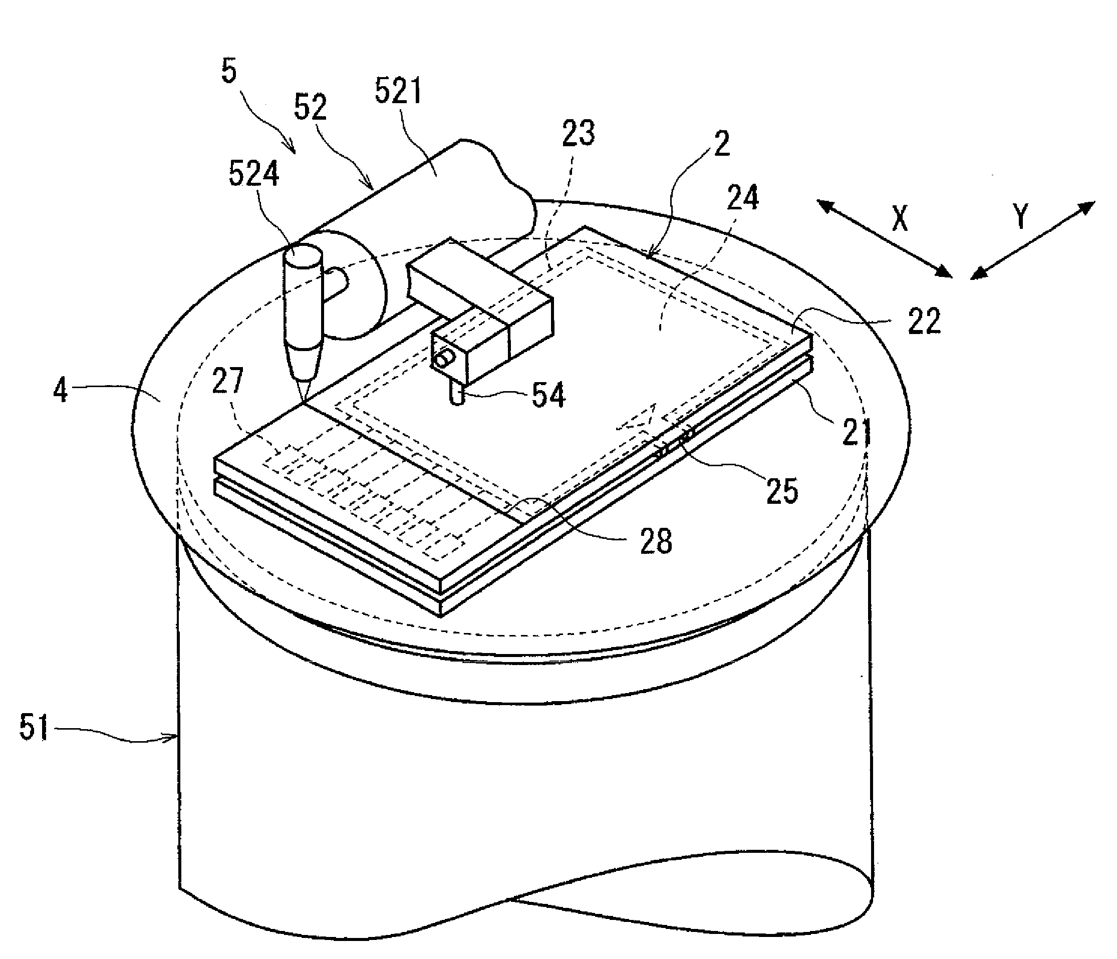
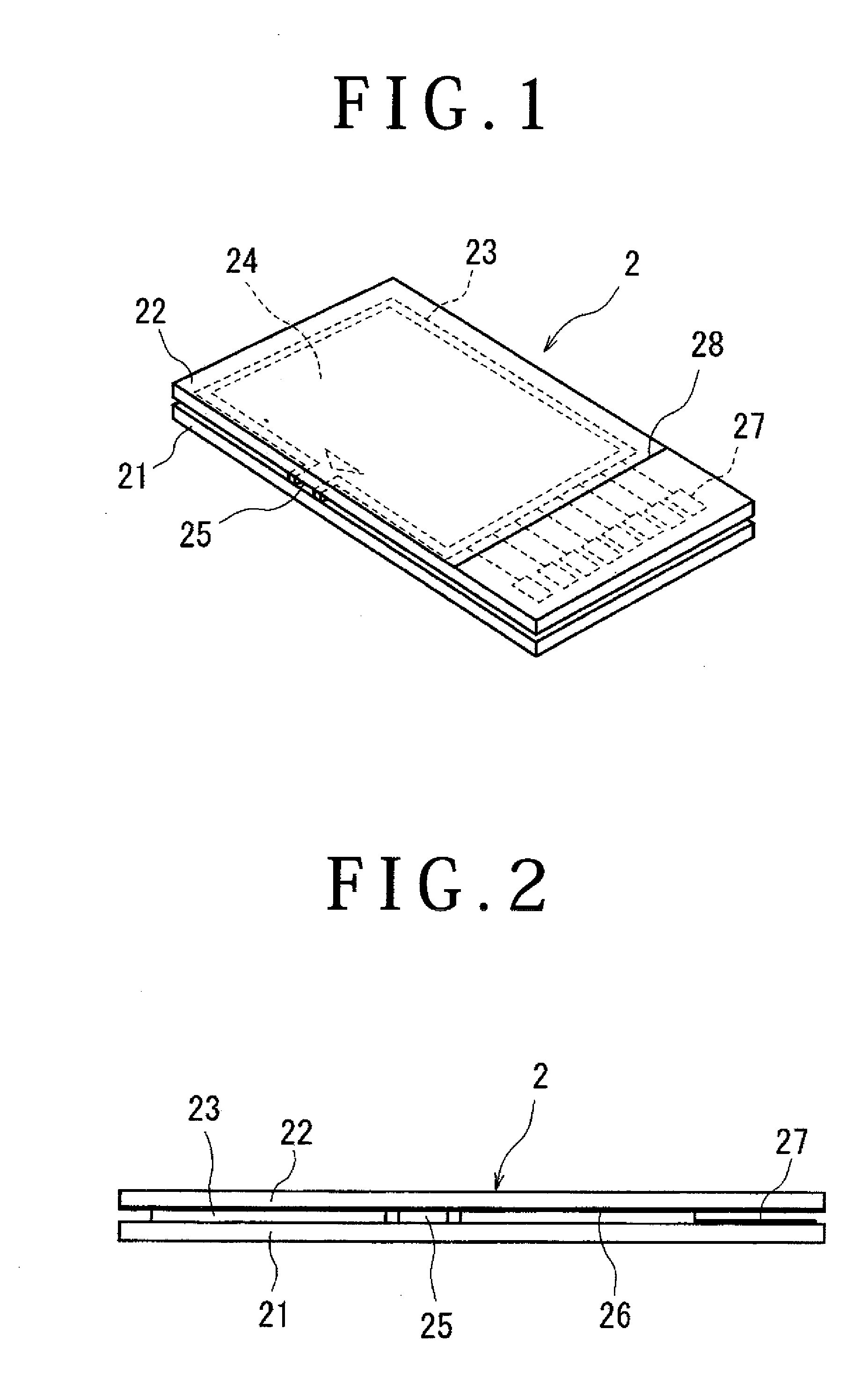
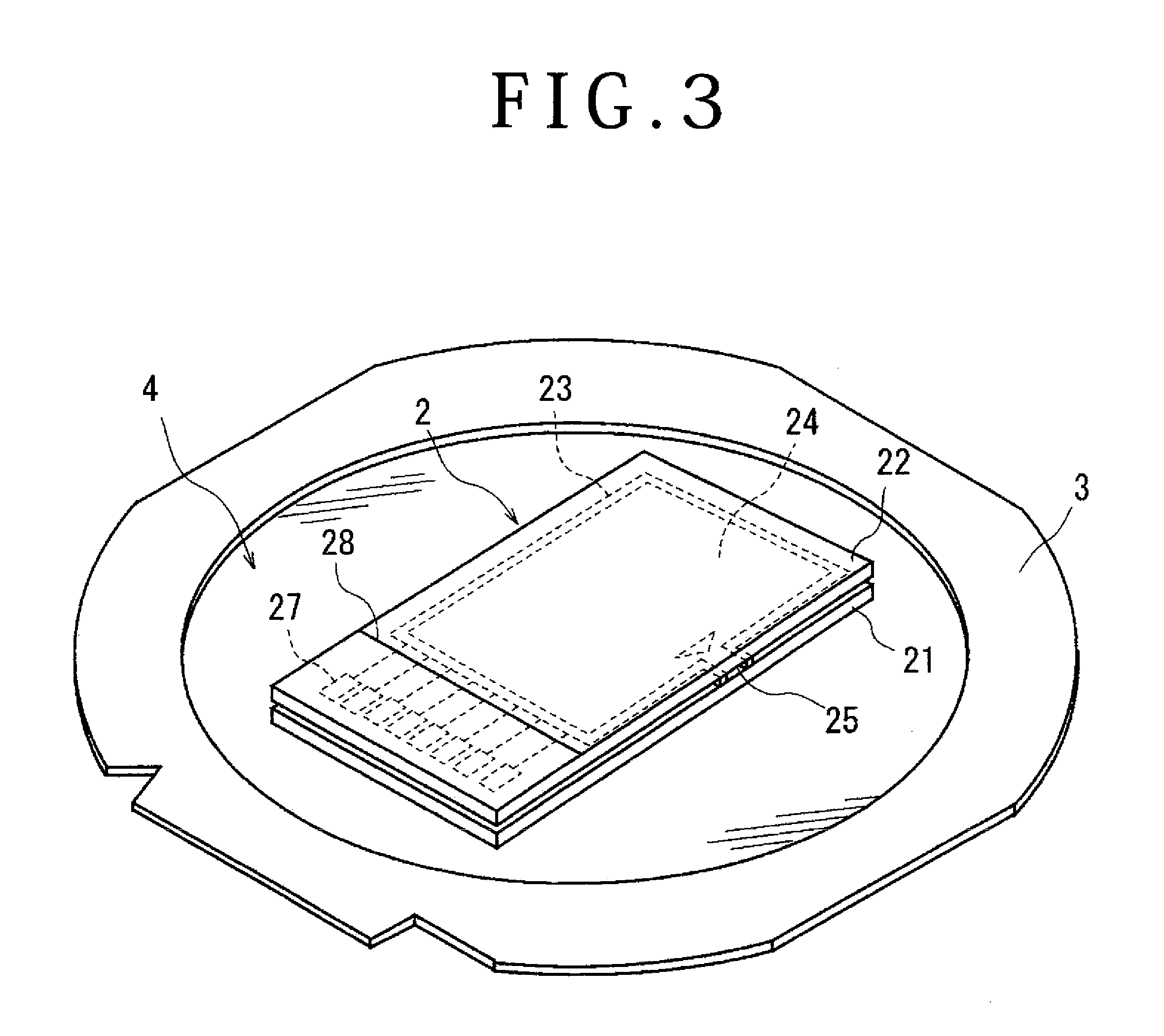
[0025]A preferred embodiment of the laser processing method according to the present invention will now be described in detail with reference to the attached drawings. FIG. 1 is a perspective view of a liquid crystal device 2 to be processed by the laser processing method according to the present invention, and FIG. 2 is a side view of the liquid crystal device 2 shown in FIG. 1. The liquid crystal device 2 shown in FIGS. 1 and 2 is composed of a silicon substrate 21 and a glass substrate 22. A liquid crystal chamber 24 is defined between the silicon substrate 21 and the glass substrate 22 so as to be surrounded by a sealing member 23. The sealing member 23 is formed with a liquid crystal filling port 25 communicating with the liquid crystal chamber 24 and opening to one end surface of the liquid crystal device 2.

[0026]A transparent conductive film 26 of indium tin oxide or the like is formed by evaporation on the inner surface of the glass substrate 22, i.e., on the surface exposed...


PUM

PropertyMeasurementUnit
repetition frequencyaaaaaaaaaa
absorption wavelengthaaaaaaaaaa

Abstract

A laser processing method for a transparent plate having a predetermined breaking line including the step of applying a pulsed laser beam to the transparent plate along the breaking line to thereby form a laser processed groove. The pulsed laser beam has an absorption wavelength to the transparent plate. The repetition frequency of the pulsed laser beam is set to 200 kHz or more and the energy density per pulse of the pulsed laser beam is set to 3.8 J / cm2 or more.

Description

BACKGROUND OF THE INVENTION[0001]1. Field of the Invention[0002]The present invention relates to a laser processing method for a transparent plate such as a glass substrate constituting a liquid crystal device, in which a laser processed groove is formed along a predetermined breaking line on the transparent plate.[0003]2. Description of the Related Art[0004]A liquid crystal device is formed by stacking a silicon substrate and a glass substrate. A liquid crystal filling port is formed on a separate surface between the silicon substrate and the glass substrate, and a liquid crystal chamber is defined between the silicon substrate and the glass substrate. A liquid crystal is filled from the liquid crystal filling port into the liquid crystal chamber. In this liquid crystal device, electrodes are formed on the inner surface of the silicon substrate, i.e., on the surface exposed to the liquid crystal chamber. These electrodes are exposed by breaking the glass substrate along a predeterm...

Claims


Application Information

Patent Timeline
Patent Type & Authority Applications(United States)
IPC IPC(8): B23K26/00B23K26/364C03B33/09G02F1/13G02F1/1333
CPCB23K26/0626B23K26/0853B23K2201/40B23K26/4075B23K26/367B23K26/364B23K26/40B23K2101/40B23K2103/50
Inventor MORIKAZU, HIROSHIHONJO, KEIJIASANO, KENJI
Owner DISCO CORP
Why Eureka
Try Eureka