Structure and method for semiconductor power devices

a technology of metal oxide semiconductor and structure, applied in semiconductor devices, diodes, electrical devices, etc., can solve the problems of limiting the switching speed of the device, affecting the efficiency of the device, so as to reduce the on-resistance, reduce the gate charge, and reduce the breakdown voltage

Active Publication Date: 2009-10-29
SEMICON COMPONENTS IND LLC
View PDF11 Cites 7 Cited by
  • Summary
  • Abstract
  • Description
  • Claims
  • Application Information

AI Technical Summary

Benefits of technology

[0008]In accordance with embodiments of the present invention, a composite semiconductor device includes an MOS transistor built in an SOI layer combined with a bipolar transistor. The drain of the MOS transistor also forms the emitter of the bipolar transistor, and the base of the bipolar transistor is coupled to the gate of the MOS transistor by a resistive element. In an embodiment, the MOS transistor is an LDMOS built in SOI for power applications. Depending on the embodiment, the composite device can provide reduced on-resistance, higher breakdown voltage, and lower gate charges. In one embodiment, part of the bipolar transistor is built in a vertical semiconductor region connecting a front side semiconductor layer of the SOI with a back side substrate. Additionally, a method for forming the composite device is provided.

Problems solved by technology

High electric fields tend to build up in the depletion region, and breakdown occurs when the electric fields exceed certain limitations.
Additionally, the charges in the well region and the body region can limit the switching speed of the device, when a gate voltage is applied to turn on and off the device.
Even though conventional LDMOS devices, such as device 100 in FIG. 1, are satisfactory in certain applications, they suffer from many limitations.
These limitations include low breakdown voltage, high on-resistance, and excess gate charges that impact device switching speed.

Method used


Image

  • Structure and method for semiconductor power devices
  • Structure and method for semiconductor power devices
  • Structure and method for semiconductor power devices

Examples


Embodiment Construction

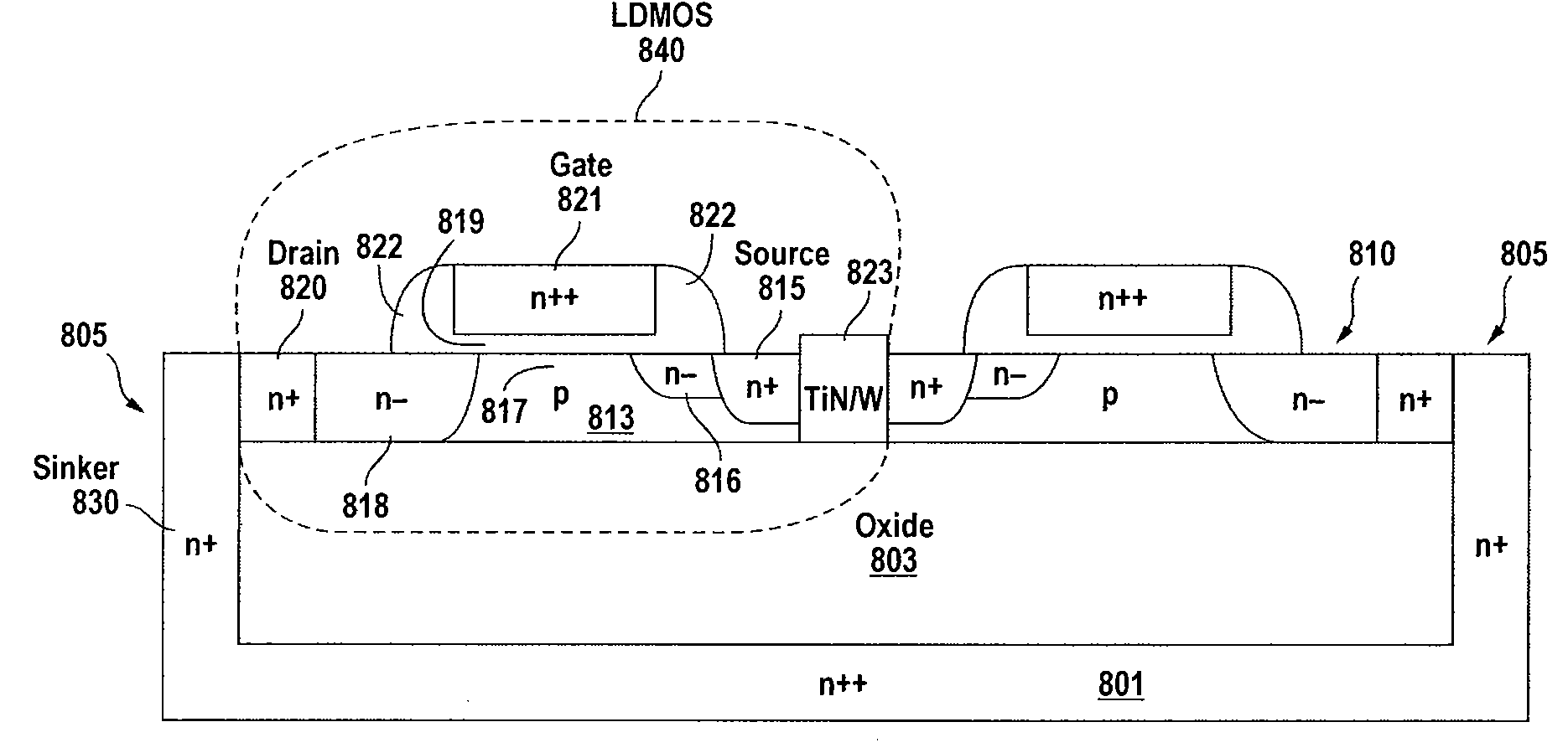
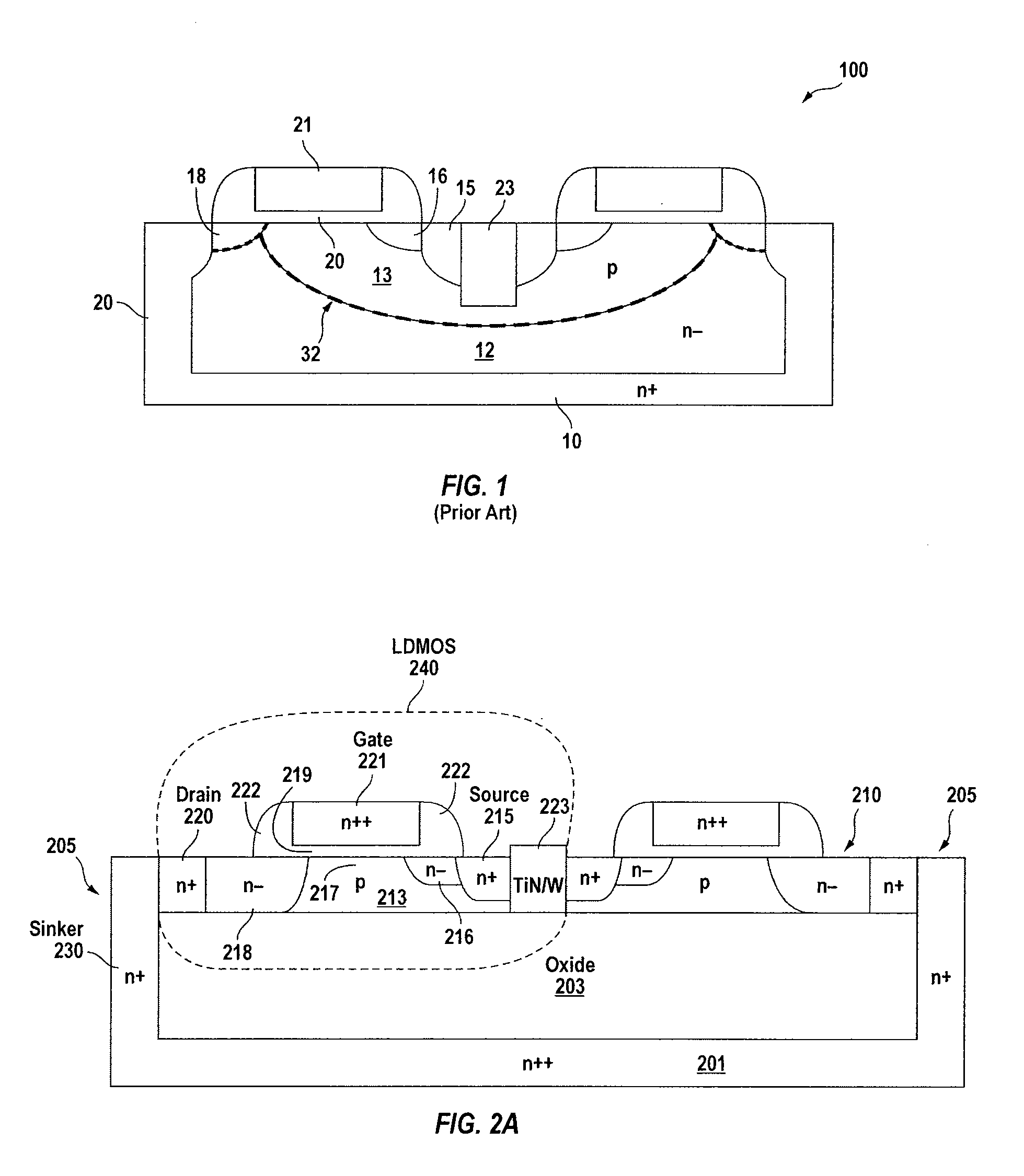
[0028]As discussed above, even though LDMOS is widely used in power applications, conventional LDMOS suffers from many limitations. For example, the gate charge can be high due to the relatively large depletion regions. Also, the breakdown voltage BVdss for LDMOS is usually limited by the p-n junctions. Additionally, Rdson in the conventional LDMOS as shown in FIG. 1 tends to be high because the current flows through a 900 path, first laterally along a surface region and then vertically into the drain at the back side of the substrate. Thus, it is desirable for LDMOS device structures and cost-effective manufacturing methods that offer improved device performance.

[0029]In accordance with embodiments of the present invention, a composite semiconductor device is provided that includes an MOS transistor built in an SOI layer combined with a bipolar transistor. The drain of the MOS transistor also forms the emitter of the bipolar transistor, and the base of the bipolar transistor is cou...


PUM


Abstract

A semiconductor device includes a semiconductor-on-insulator region on a substrate. The semiconductor-on-insulator region includes a first semiconductor region overlying a dielectric region. The device includes an MOS transistor and a bipolar transistor. The MOS transistor has a drain region, a body region, and a source region in the first semiconductor region. The MOS transistor also includes a gate. The device also includes a second semiconductor region overlying the substrate and adjacent to the drain region, and a third semiconductor region overlying the substrate and adjacent to the second semiconductor region. The bipolar transistor includes has the drain region of the MOS transistor as an emitter, the second semiconductor region as a base, and the third semiconductor region as a collector. Accordingly, the drain of the MOS transistor also functions as the emitter of the bipolar transistor. Additionally, the gate and the base are coupled by a resistive element.

Description

BACKGROUND OF THE INVENTION[0001]The present invention relates in general to semiconductor power devices. More particularly, the invention provides structures and methods for a high voltage laterally diffused metal oxide semiconductor (LDMOS) device.[0002]High voltage LDMOS transistors are finding increasingly broad applications in modern electronics, such as portable consumer electronics, power management circuits, automotive electronics, disk drives, display devices, RF communication circuits, and wireless base station circuits, etc. In these applications, the performance of an LDMOS transistor is usually measured by its on-resistance, switching speed, and breakdown voltage.[0003]FIG. 1 is a cross-sectional view of a conventional high voltage LDMOS transistor 100. An n-type well region 12 is formed on an n-type substrate 10. A p-type body region 13 is formed in n-type well region 12. An n+-type source region 15 and an n-type lightly doped source region 16 are formed in p-type body...

Claims


Application Information

Patent Timeline
Patent Type & Authority Applications(United States)
IPC IPC(8): H01L29/00H01L21/8249
CPCH01L21/743H01L21/8249H01L21/84H01L29/7835H01L27/0635H01L27/1203H01L29/1087H01L27/0623H01L29/4175H01L29/78624
Inventor PAN, JAMES
Owner SEMICON COMPONENTS IND LLC
Why Eureka
Try Eureka