Semiconductor Device and Method for Fabricating the Same

Active Publication Date: 2009-10-29
SK HYNIX INC
View PDF4 Cites 7 Cited by
  • Summary
  • Abstract
  • Description
  • Claims
  • Application Information

AI Technical Summary

Benefits of technology

[0020]Various embodiments of the present invention are directed to providing a semiconductor device and a method for fabricating the same. In the method, the upper portion of a landing plug is preferably formed to be broader than the lower portion of the landing plug in the ma

Problems solved by technology

Recently, data storage capacity of the semiconductor memory apparatus has increased, but the size of the semiconductor memory apparatus has not increased proportionally.
As a result, a refresh operation is periodically required on the unit cells so that data of the DRAM cannot be destroyed.
As the design rule is reduced, the plane area where a capacitor can be formed is reduced, and it is difficult to develop materials for constituting an insulating film in the capacitor.
As a result, the junction resistance value of the storage node (SN) and the turn-on resistance value of the transistor in the unit cell are greater, it is difficult to perform normal read and write operations, and refresh characteristics are deteriorated.
However, it is difficult to prevent reduction of the number of holes that the floating body of the transistor stores because of the leakage current that occurs at the source line junction or t

Method used


Image

  • Semiconductor Device and Method for Fabricating the Same
  • Semiconductor Device and Method for Fabricating the Same
  • Semiconductor Device and Method for Fabricating the Same

Examples


Embodiment Construction

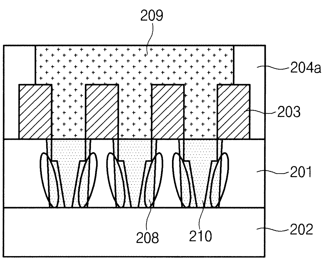
[0045]FIG. 2a to 2g are cross-sectional diagrams illustrating a method for manufacturing a floating body transistor in a semiconductor memory apparatus according to an embodiment of the present invention.

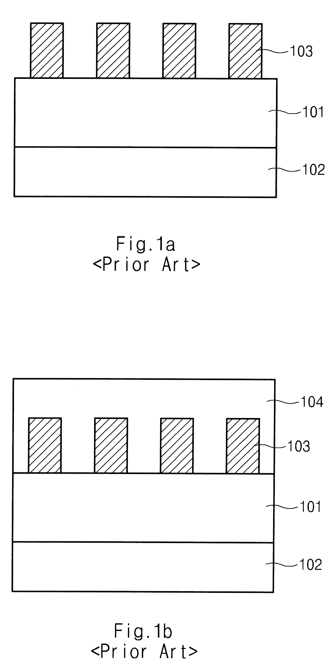
[0046]Referring to FIG. 2a, a gate pattern 203 including a gate electrode and a hard mask for protecting the gate electrode is formed over a silicon active region 201. Impurities are doped between the gate patterns 203 to form a lightly doped drain (LDD) (not shown). According to an embodiment, a semiconductor memory apparatus including a floating body transistor is preferably fabricated with a silicon-on-insulator (SOI) wafer including a lower insulating oxide layer 202 and the silicon active region 201 formed over the lower insulating oxide layer 202.

[0047]Referring toFIG. 2b, an interlayer dielectric (ILD) oxide film 204 is formed over the resulting structure including the gate pattern 203.

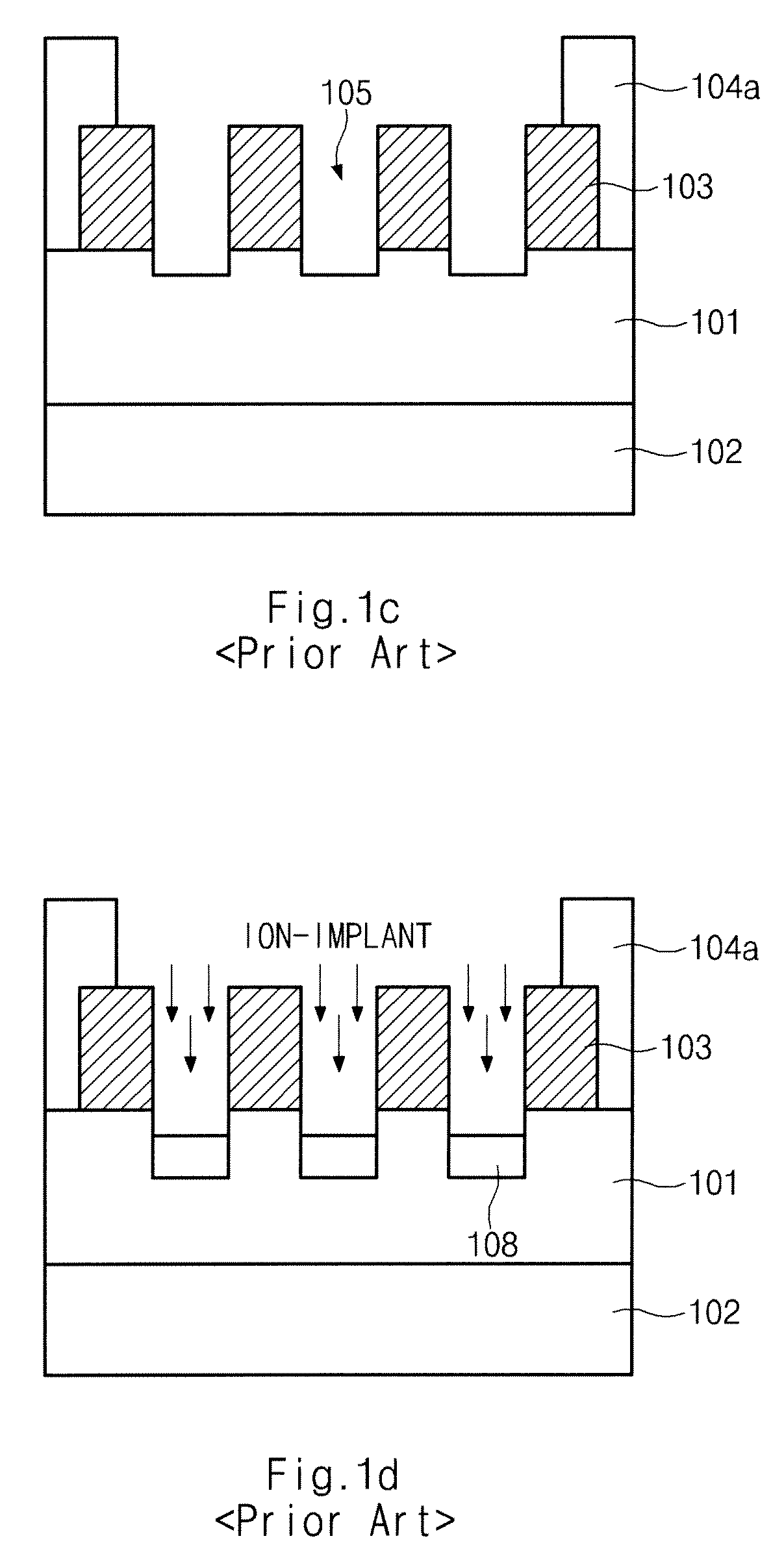
[0048]Referring to FIG. 2c, to form a self-aligned contact (SAC), the ILD oxide film 204 is...


PUM


Abstract

A method for fabricating a semiconductor device comprises: forming a gate pattern over a silicon active region and an insulating layer, which form a semiconductor substrate; removing the silicon active region exposed between the gate patterns; and filling a space between the gate patterns to form a plug.

Description

CROSS-REFERENCES TO RELATED APPLICATIONS[0001]Priority to Korean patent application number 10-2008-0038345, filed on Apr. 24, 2008, which is incorporated by reference in its entirety, is claimed.BACKGROUND OF THE INVENTION[0002]The present invention relates generally to a method for fabricating a semiconductor device, and more specifically, to a method of forming a floating body transistor used in a highly-integrated semiconductor device using a silicon-on-insulator (SOI) substrate.[0003]In a system containing a plurality of semiconductor devices, a semiconductor memory apparatus is configured to store data generated or processed therein. For example, if a request from a data processor such as a central processing unit (CPU) is received, the semiconductor memory apparatus outputs data to the data processor from unit cells therein or stores data processed by the data processor to the unit cells, according to an address transmitted with the request.[0004]Recently, data storage capacit...

Claims


Application Information

Patent Timeline
IPC IPC(8): H01L29/786H01L21/84H01L21/302H01L21/311
CPCH01L27/108H01L29/7841H01L27/10802H10B12/20H10B12/00H01L21/265H01L21/28141H01L21/76229H01L21/76838
Inventor CHUNG, SU OCK
Owner SK HYNIX INC
Why Eureka
Try Eureka