Illuminating device

a technology of illumination device and discharge tube, which is applied in the direction of discharge tube/lamp details, luminescent compositions, discharge tube luminescnet screens, etc., can solve the problems of complicated illumination device, and achieve the effect of low color rendering properties and complicated illumination devi

Inactive Publication Date: 2009-10-29
CMC MAGNETICS CORPORATION
View PDF4 Cites 53 Cited by
  • Summary
  • Abstract
  • Description
  • Claims
  • Application Information

AI Technical Summary

Benefits of technology

[0010]The present invention has been made in view of the above mentioned problems and it is an object thereof to provide an illuminating device having a simple structure without using extra optical members such as the lens and shading member with a specific structure, not producing unevenness or rings in color or brightness on the irradiation face, and having excellent uniformity in light emission and excellent property in color rendering.
[0029]According to the present invention, by defining the excitation light contribution ratio ΔE as described above, the light generated from the semiconductor light emitting element is scarcely emitted and the light generated from the phosphor in the luminescent part is mostly emitted. Therefore, the illuminating device can be provided, which has a simple structure without using particular optical members, not produces unevenness or rings in color or brightness on the irradiation face, and has excellent uniformity in light emission. Furthermore, the illuminating device having excellent property in color rendering can be provided because it has the mean color rendering index Ra of 70 or more.

Problems solved by technology

However, in Patent References 1 and 2, the illuminating devices are complicated because they have extra lens and shading member with a specific structure.

Method used


Image

  • Illuminating device
  • Illuminating device
  • Illuminating device

Examples


examples

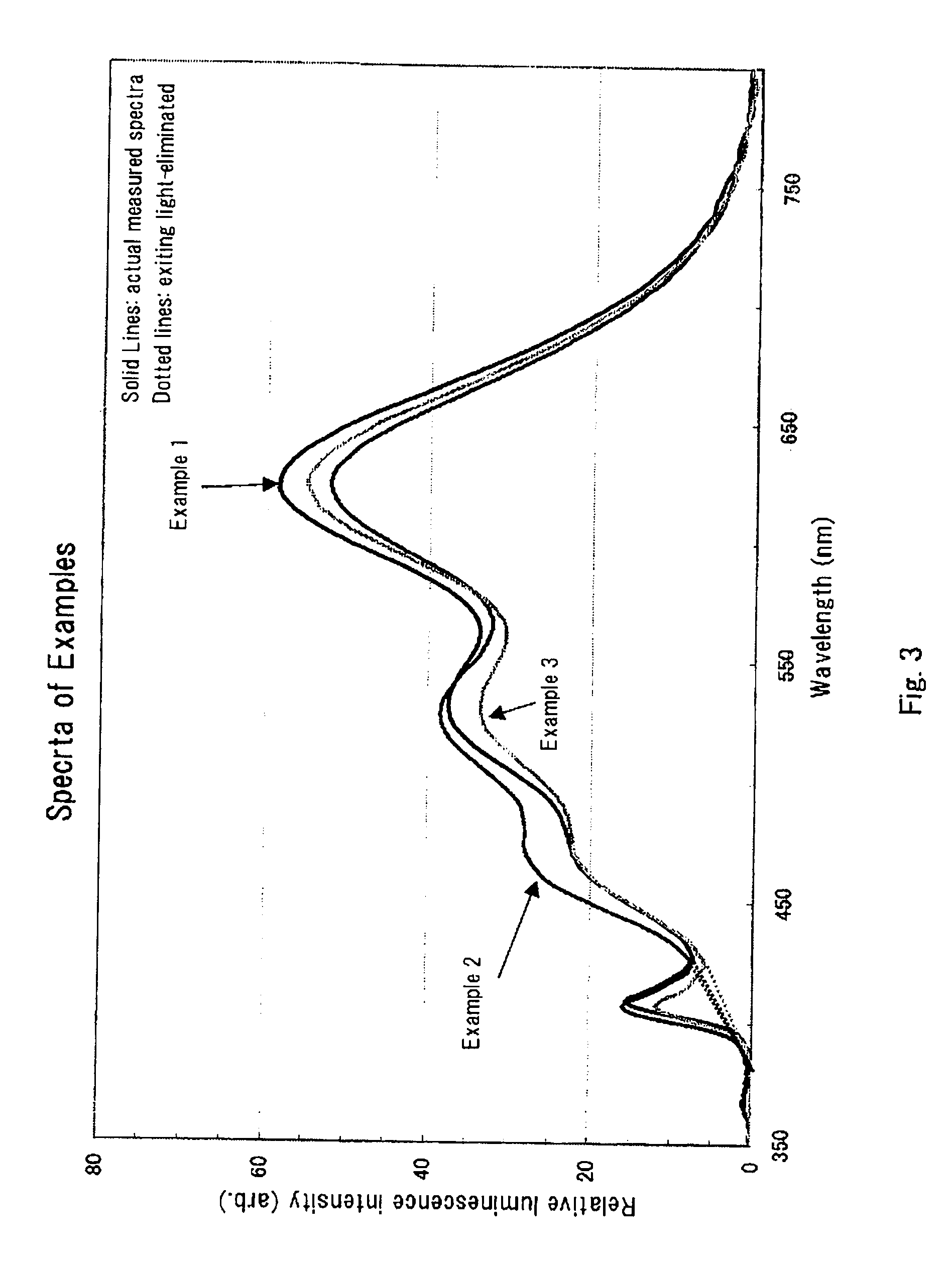
[0319]Hereinafter, the present invention is more specifically explained with examples; however, the present invention is not limited by the following examples unless exceeding its scope.

[0320]The following luminescent device was manufactured and assessed by using the following as the semiconductor light emitting element, sealing member and phosphor.

[0321]

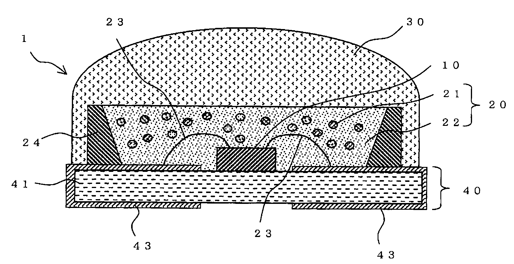
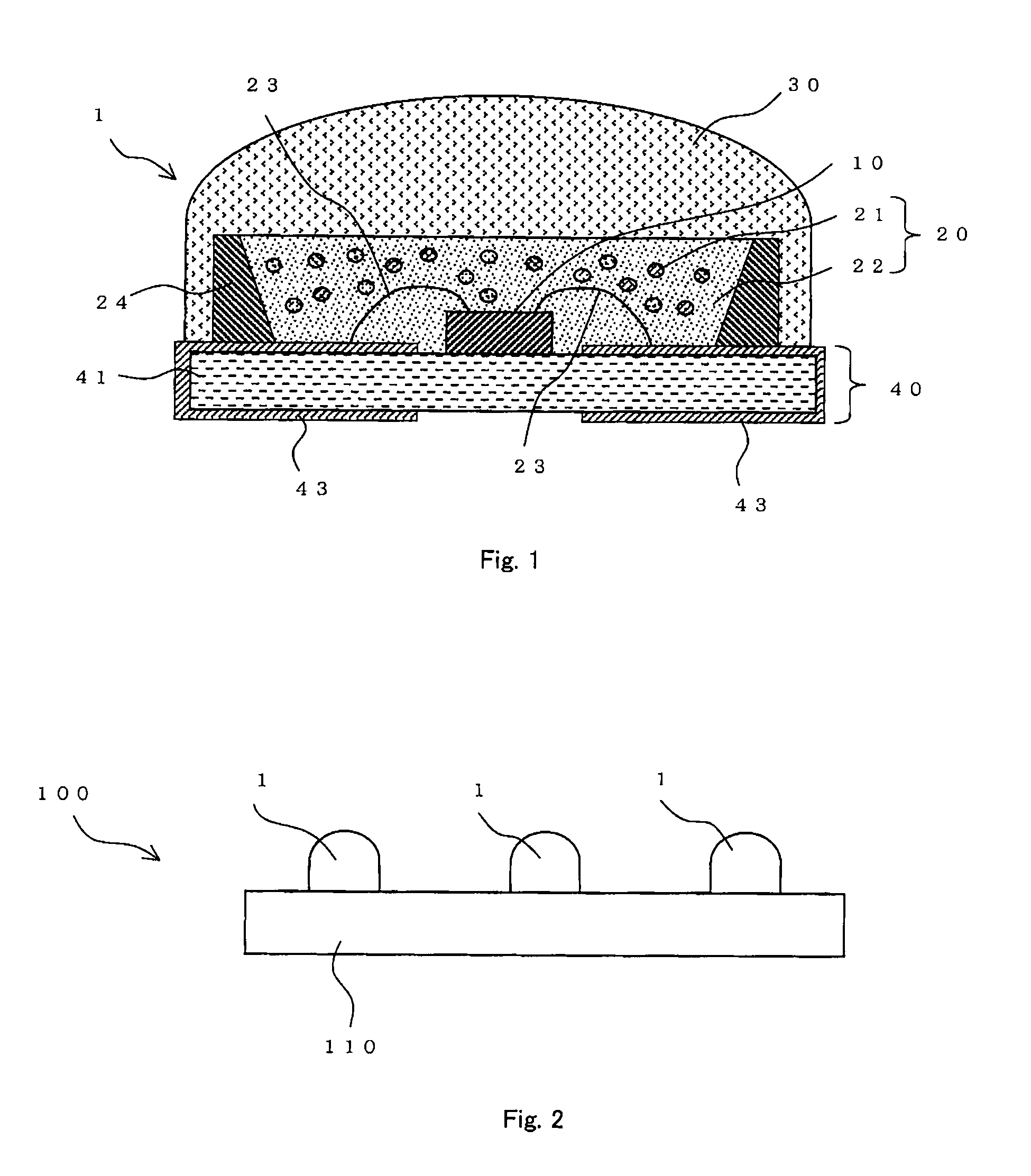
[0322]As the semiconductor light emitting element (hereinafter referred to as “chip”), a GaN-based light emitting diode (LED) with a peak wavelength of 405 nm, a full width at half maximum of 30 nm, and a square-shaped size of 350 μm and 350 μm was used.

[0323]

[0324]50 g of both-ends silanol dimethyl silicone oil (manufactured by Toshiba Silicones Co., Ltd., XC96-723), 5.0 g of phenyltrimethoxysilane, and 11 g of zirconium tetra-n-propoxide solution as a catalyst (5 parts by weight of 75% by weight of solution of zirconium tetra-n-propoxide in n-propanol was diluted with 95 parts by weight of toluene) were stirred at the room tempera...


PUM


Abstract

An illuminating device comprises one or more luminescent devices (1). The luminescent device comprises a semiconductor light emitting element (10) emitting a excitation light having an peak within a wavelength range from 350 nm to 430 nm, and a luminescent part (20) comprising a sealing member (22) and a phosphor (21) absorbing the light from the semiconductor light emitting element (10) and emitting a light with different emission spectrum. For the luminescent device (1), an excitation light contribution degree ΔE, an index quantitatively representing what extent of a visible component of the excitation light is involved in color mixing of a combined light of the luminescent device (1), is 0.005 or less, and a mean color rendering index Ra is 70 or more.

Description

TECHNICAL FIELD[0001]The present invention relates to a illuminating device using a semiconductor light emitting element such as a light emitting diode (LED). Particularly, the present invention relates to a white colors- or pastel colors-illuminating device where a plurality of LEDs are integrated.BACKGROUND ART[0002]For an illuminating device such as an LED lamp using a semiconductor light emitting element, the surface of the semiconductor light emitting element is coated with a phosphor, or powder of the phosphor is contained in the resin constructing the LED lamp to practically realize other emission colors, for example white, than the original emission color from the semiconductor light emitting element. In such illuminating device, the GaN-based semiconductor light emitting element emitting blue light with a center wavelength approximately 460 nm is generally utilized. More specifically, the surface of the GaN-based semiconductor light emitting element emitting blue light is c...

Claims


Application Information

Patent Timeline
Patent Type & Authority Applications(United States)
IPC IPC(8): H01J1/63H01L33/50
CPCC09K11/0883C09K11/7734H01L33/50H01L2224/48091H01L2224/45144H01L2924/00014H01L2924/00H01L2924/181C09K11/77342H01L2924/00012
Inventor KASAKURA, AKEOKAGAWA, KAZUHIKOKIJIMA, NAOTO
Owner CMC MAGNETICS CORPORATION
Why Eureka
Try Eureka