Semiconductor device including a plurality of chips and method of manufacturing semiconductor device

a semiconductor device and semiconductor technology, applied in semiconductor devices, semiconductor/solid-state device details, electrical devices, etc., can solve the problem of difficult reduction of substrate dimensions, and achieve the effect of reducing the dimension of semiconductor devices

Inactive Publication Date: 2009-11-12
DENSO CORP
View PDF21 Cites 31 Cited by
  • Summary
  • Abstract
  • Description
  • Claims
  • Application Information

AI Technical Summary

Benefits of technology

[0010]In the semiconductor device according to the first aspect, the first chip and the second chip can be integrated by attaching the second-surface drain electrode of the first chip to the second-surface drain electrode of the second chip. Thus, a lead frame is not required to be disposed between the first chip and the second chip. Therefore, a dimension of the semiconductor device can be reduced compared with a case where the lead frame is disposed.
[0013]In the semiconductor device according to the second aspect, the first chip and the second chip can be integrated by attaching the second-surface drain electrode of the first chip to the source electrode of the second chip. Thus, a lead frame is not required to be disposed between the first chip and the second chip. Therefore, a dimension of the semiconductor device can be reduced compared with a case where the lead frame is disposed.
[0016]In the semiconductor device according to the third aspect, the first chip and the second chip can be integrated by attaching the emitter electrode of the first chip to the source electrode of the second chip. Thus, a lead frame is not required to be disposed between the first chip and the second chip. Therefore, a dimension of the semiconductor device can be reduced compared with a case where the lead frame is disposed.
[0019]In the semiconductor device according to the fourth aspect, the first chip and the second chip can be integrated by attaching the second surface of the first chip to the source electrode of the second chip. Thus, a lead frame is not required to be disposed between the first chip and the second chip. Therefore, a dimension of the semiconductor device can be reduced compared with a case where the lead frame is disposed.

Problems solved by technology

Thus, when a plurality of power devices is formed on one plane of a chip or when a plurality of power devices is formed on respective chips and the chips are arranged on one plane, a dimension of a substrate is difficult to be reduced.

Method used


Image

  • Semiconductor device including a plurality of chips and method of manufacturing semiconductor device
  • Semiconductor device including a plurality of chips and method of manufacturing semiconductor device
  • Semiconductor device including a plurality of chips and method of manufacturing semiconductor device

Examples


first embodiment

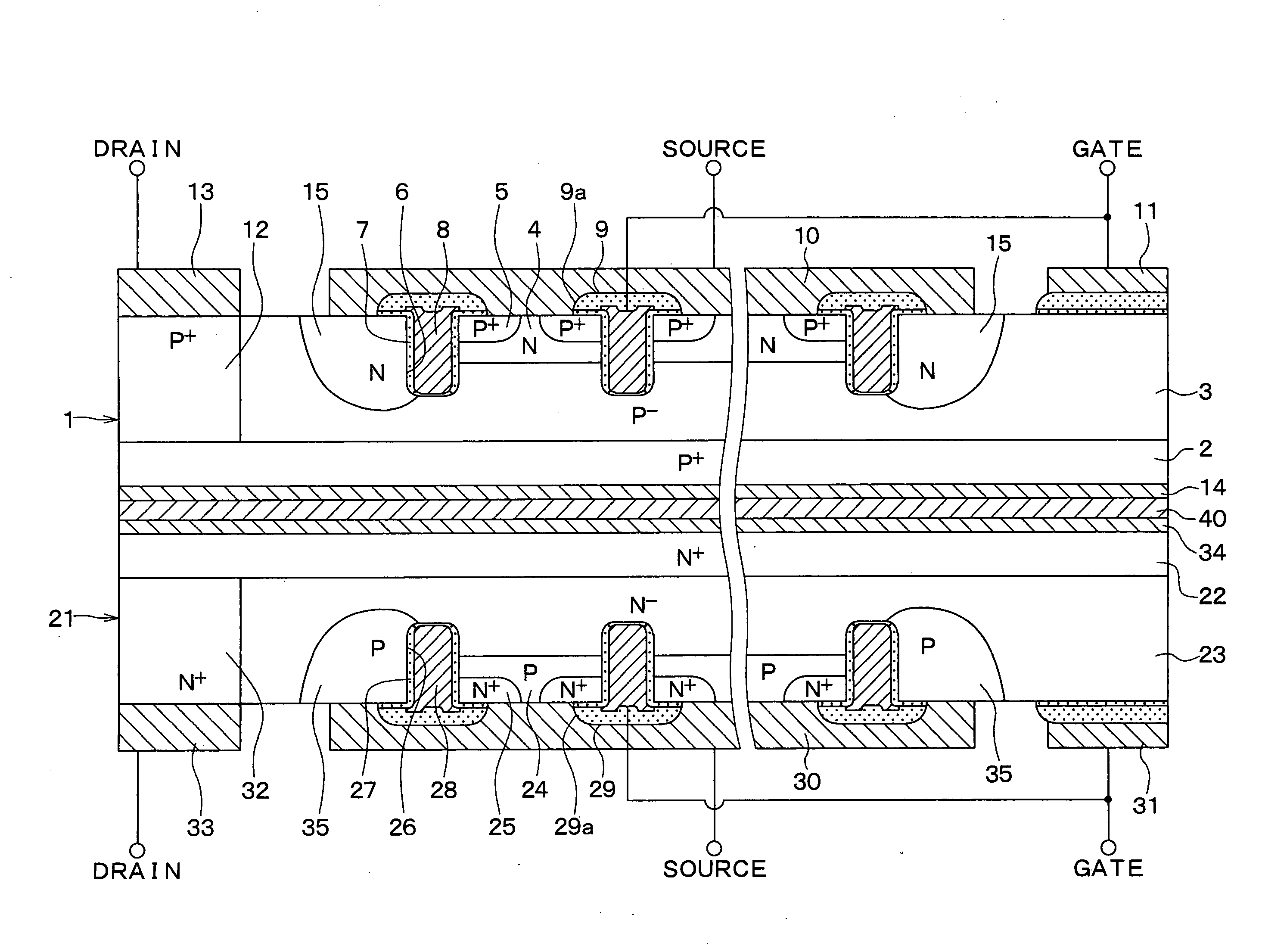
[0039]A semiconductor device according to a first embodiment of the present invention will be described with reference to FIG. 1 and FIG. 2.

[0040]The semiconductor device includes a first chip 1 and a second chip 21. Each of the first chip 1 and the second chip 21 includes a power MOSFET having a trench gate structure as a vertical power device. A second surface of the first chip 1 is attached to a second surface of the second chip 21 so that the first chip 1 is integrated with the second chip 2.

[0041]The first chip 1 includes a P channel power MOSFET. The first chip 1 includes a P+ type silicon substrate 2. The P+ type silicon substrate 2 has first and second opposing surfaces. On the first surface of the P+ type silicon substrate 2, a P− type drift layer 3 is epitaxially formed. The P− type drift layer 3 has a cell section. An N type channel layer 4 is disposed at a surface portion of the cell section of the P− type drift layer 3. A P+ type source region 5 is disposed at a surface...

second embodiment

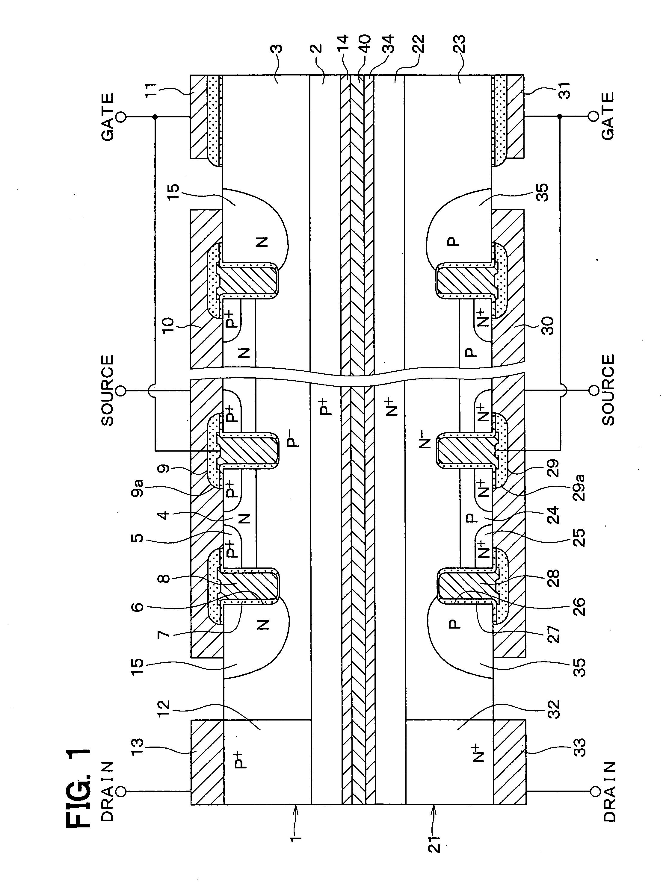
[0056]A semiconductor device according to second embodiment of the present invention will be described with reference to FIG. 5 and FIG. 6. In the semiconductor device according to the first embodiment, the first chip 1 includes the P channel power MOSFET and the second chip 21 includes the N channel power MOSFET. In the semiconductor device according to the present embodiment, both of the first chip 1 and the second chip 21 includes a P channel MOSFET.

[0057]The P channel MOSFETs in the first chip 1 and the second chip 21 of the present embodiment are similar to the P channel MOSFET in the first chip 1 of the first embodiment. However, in the present embodiment, the first chip 1 and the second chip 21 do not have the up-drain structure. Thus, the P+ type contact layer 12 and the first-surface drain electrode 13 illustrated in FIG. 1 are not provided.

[0058]The second-surface drain electrode 14 of the first chip 1 is electrically coupled with the source electrode 10 of the second chip...

third embodiment

[0065]A semiconductor device according to a third embodiment of the present invention will be described with reference to FIG. 9 and FIG. 10.

[0066]The semiconductor according to the present embodiment includes a first chip 1 and a second chip 21. The first chip 1 includes an N channel IGBT. The second chip 21 includes an N channel power MOSFET. The N channel power MOSFET in the second chip 21 according to the present embodiment is similar to the N channel power MOSFET in the second chip 21 according to the first embodiment. However, in the present embodiment, the second chip 21 does not have the up-drain structure. Thus, the N+ type contact layer 32 and the first-surface drain electrode 33 illustrated in FIG. 1 are not provided.

[0067]The N channel IGBT formed in the first chip 1 includes a P+ type silicon substrate 51. On a first surface of the P+ type silicon substrate 51, an N+ type buffer layer 52 and an N− type drift layer 53 are epitaxially formed. The N− type drift layer 53 in...


PUM


Abstract

A semiconductor device includes a first chip and a second chip. The first chip includes a first conductivity type channel power MOSFET. The second chip includes a second conductivity type channel power MOSFET. The first chip and the second chip are integrated in such a manner that a second-surface drain electrode of the first chip and a second-surface drain electrode of the second chip face to each other and are electrically coupled with each other through a conductive material.

Description

CROSS REFERENCE TO RELATED APPLICATIONS[0001]The present application is based on and claims priority to Japanese Patent Applications No. 2008-122149 filed on May 8, 2008, and No. 2009-050455 filed on Mar. 4, 2009, the contents of which are incorporated in their entirety herein by reference.BACKGROUND OF THE INVENTION[0002]1. Field of the Invention[0003]The present invention relates to a semiconductor device including a plurality of chips. The present invention also relates to a method of manufacturing a semiconductor device.[0004]2. Description of the Related Art[0005]Conventionally, a power device such as a power metal-oxide semiconductor field-effect transistor (power MOSFET) and an insulated gate bipolar transistor (IGBT) is used for driving a load such as a motor. In a case where a full bridge circuit is assembled from power devices for driving a motor, four power devices are required for driving a brush motor and six power devices are required for driving a brushless motor. Thu...

Claims


Application Information

Patent Timeline
Patent Type & Authority Applications(United States)
IPC IPC(8): H01L29/739H01L29/78H01L23/495H01L21/50H01L21/336H01L21/8234H01L25/065H01L25/07H01L25/18H01L27/088H01L29/423H01L29/49
CPCH01L25/074H01L25/50H01L2924/1305H01L2924/1306H01L2225/06562H01L2224/97H01L2224/94H01L2224/32145H01L24/97H01L24/94H01L24/95H01L2924/13091H01L2924/13055H01L2924/00H01L2224/83H01L2224/04026H01L2224/04042H01L2224/06181
Inventor OZOE, SHOJI
Owner DENSO CORP
Why Eureka
Try Eureka