Electromigration-Complaint High Performance FET Layout

a high-performance, fet technology, applied in the direction of semiconductor devices, semiconductor/solid-state device details, conductors, etc., can solve the problems of cmos device fsub>t /sub> and fsub>max /sub>, and the reliability of em is affected, and the ics fails

Inactive Publication Date: 2009-11-12
GLOBALFOUNDRIES INC
View PDF14 Cites 63 Cited by
  • Summary
  • Abstract
  • Description
  • Claims
  • Application Information

AI Technical Summary

Problems solved by technology

As is well known, fT and fMAX for a CMOS device are mainly limited by the parasitic components associated with the devices gate, source and drain connections in addition to the intrinsic transit time from source to drain across the device channel.
Connections to devices in ICs, for example, connections to an FET device, will operate at relatively large current densities and may face electromigration (EM) reliability issues.
When electrical current flows through metal conductors or interconnections, EM or current limiting mechanisms due to heat may occur, causing failure of ICs.
This may cause disconnection of the interconnection or an open circuit.
As the cross-section of metal interconnects becomes smaller with technology scaling, current density becomes larger for a given amount of current being carried, and EM becomes more severe.

Method used


Image

  • Electromigration-Complaint High Performance FET Layout
  • Electromigration-Complaint High Performance FET Layout
  • Electromigration-Complaint High Performance FET Layout

Examples


Embodiment Construction

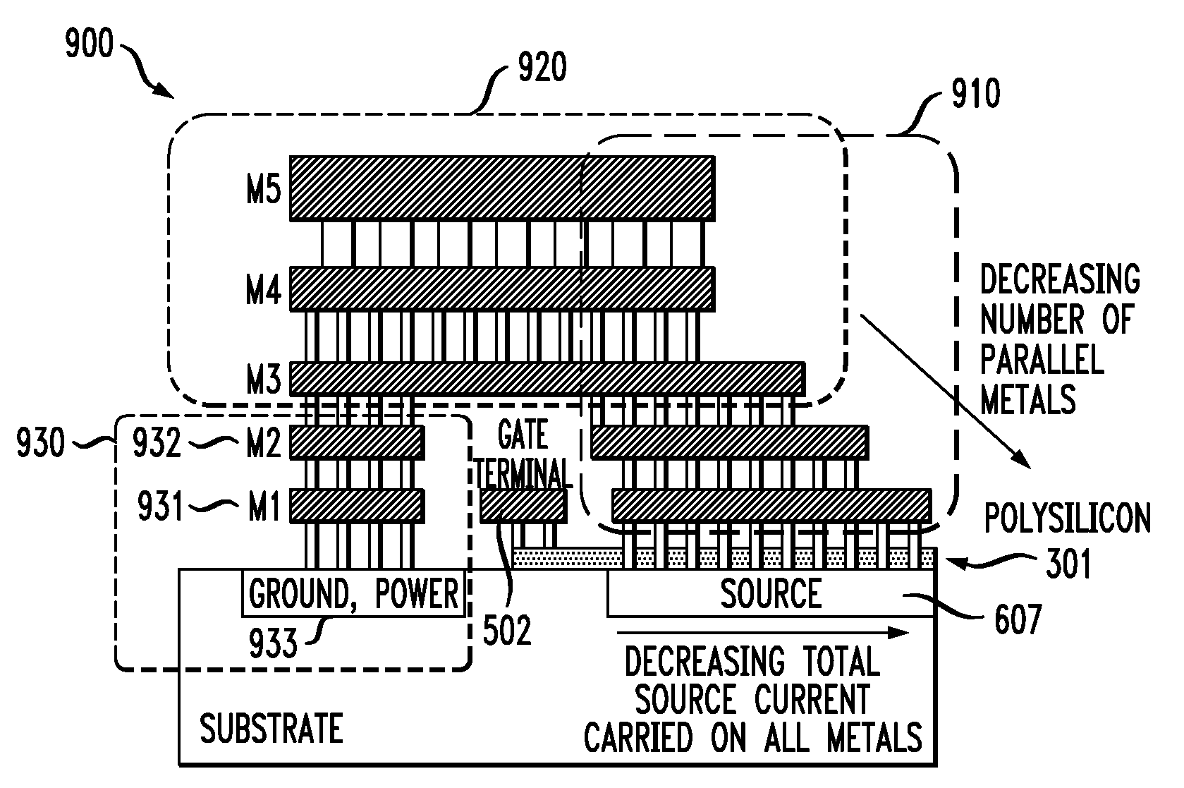
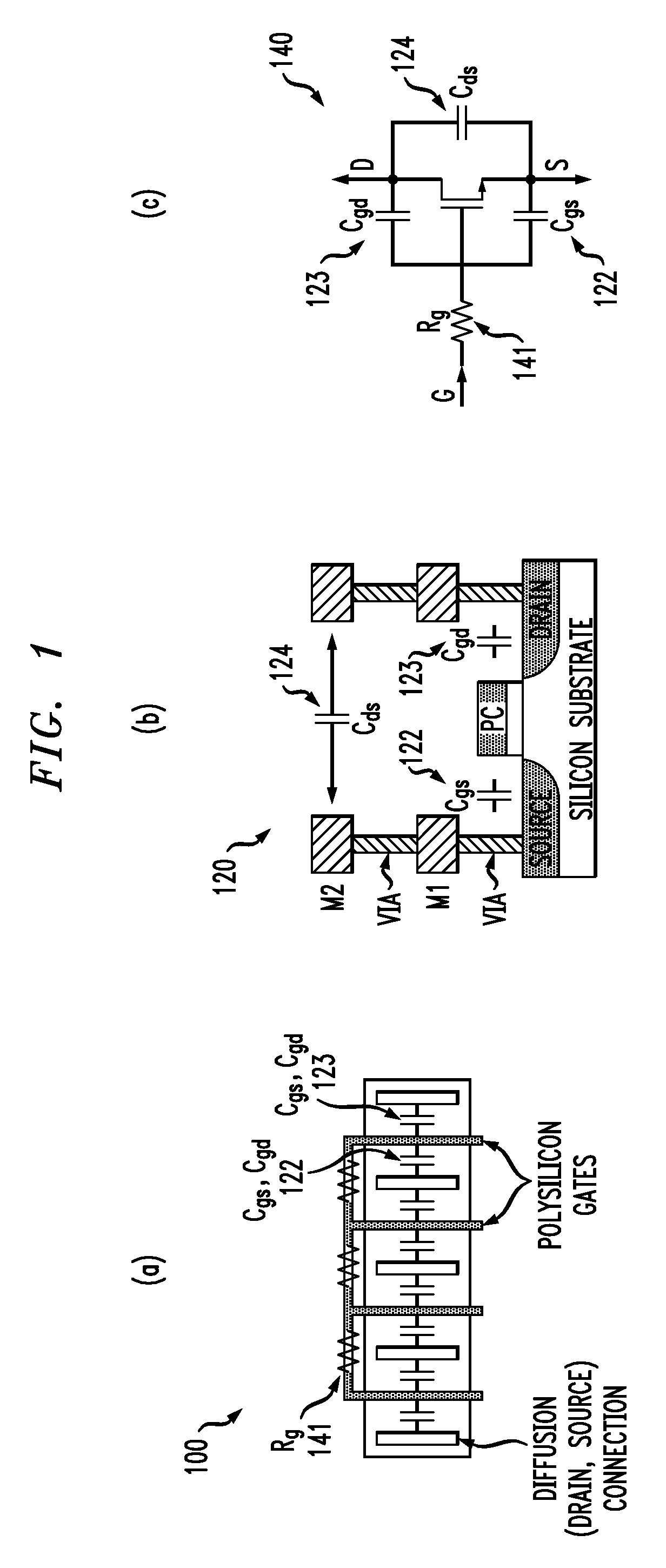
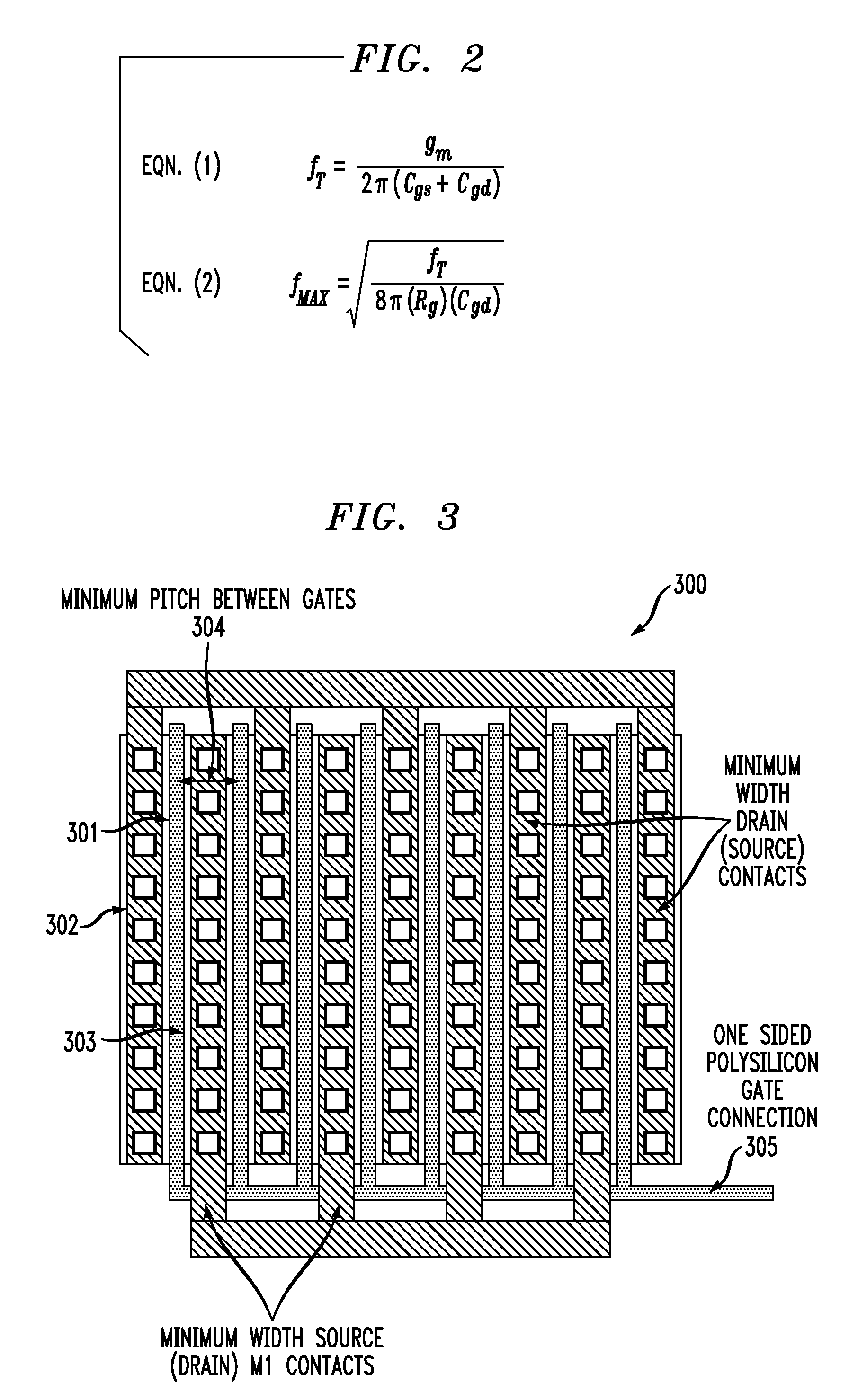
[0028]It is well known in the art that IC are fabricated with many levels of metal used for interconnect or signal or power supply routing. All metal levels are substantially in planes above and parallel to the surface of the silicon. The lowest level metal will be closest to the surface of the silicon, and the highest level of metal furthest away, with intermediate levels between. Metal connectors, interconnects and runners are terms used to indicate a route of metal used as a connection. These connectors, interconnects and runners are typically constructed form one or more rectangular features, typically but not necessarily, long and narrow. Metal connectors, interconnects and runners may be constructed on multiple levels of metal, sometimes having similar shape and size rectangles over or partially over, that is overlapping or partially overlapping, each other with vertical connections, called vias, physically located between and connecting overlapping features on different metal...


PUM

PropertyMeasurementUnit
Rgaaaaaaaaaa
lengthaaaaaaaaaa
widthaaaaaaaaaa

Abstract

An electrical contact structure distributes current along a length thereof. The electrical contact structure includes a plurality of n metal rectangles on n levels of metal. The rectangle on one metal level is at least as wide in width and vertically covers in width the rectangle on the metal level immediately below. The rectangle on one metal level is shorter in length than and substantially aligned at a first end with the rectangle on the metal level immediately below. Rectangle first ends are substantially aligned. Features of an exemplary FET transistor of this invention are a source and drain terminal electrical contact structure, a multi-level metal ring connecting gate rectangles on both ends, and a wider-than-minimum gate-to-gate spacing. The invention is useful, for example, in an electromigration-compliant, high performance transistor.

Description

[0001]This invention was made with Government support under Contract Nos.: N66001-05-C-8013 and N66001-02-C-8014 awarded by the DARPA —Defense Advanced Research Project Agency. The Government has certain rights in this invention.FIELD OF THE INVENTION[0002]The present invention relates generally to semiconductor devices and integrated circuits (ICs) and, more particularly, the invention relates to the layout of field effect transistors (FET) implemented in complementary metal oxide semiconductor (CMOS) technology.BACKGROUND OF THE INVENTION[0003]CMOS technology is receiving increasing attention for radio frequency and millimeter wave (mmWave) applications due to integration of digital processors and memory circuits with RF circuits. Cut-off frequency (fT) and maximum oscillation frequency (fMAX) are recognized as performance figures-of-merit for semiconductor devices. fT is the frequency at which the forward small-signal, short-circuit current gain of an active device has a value of...

Claims


Application Information

Patent Timeline
Patent Type & Authority Applications(United States)
IPC IPC(8): H01L29/78H01B5/00
CPCH01L23/4824H01L29/4238H01L29/78H01L2924/14H01L2924/0002H01L2924/30105H01L2924/00H01L21/768H01L27/0207H01L29/42376H01L27/088H01L29/41758H01L23/528
Inventor GREENBERG, DAVID ROSSPLOUCHART, JEAN-OLIVIERVALDES-GARCIA, ALBERTO
Owner GLOBALFOUNDRIES INC
Why Eureka
Try Eureka