LCD device based on dual source drivers with data writing synchronous control mechanism and related driving method
- Summary
- Abstract
- Description
- Claims
- Application Information
AI Technical Summary
Benefits of technology
Problems solved by technology
Method used
Image
Examples
first embodiment
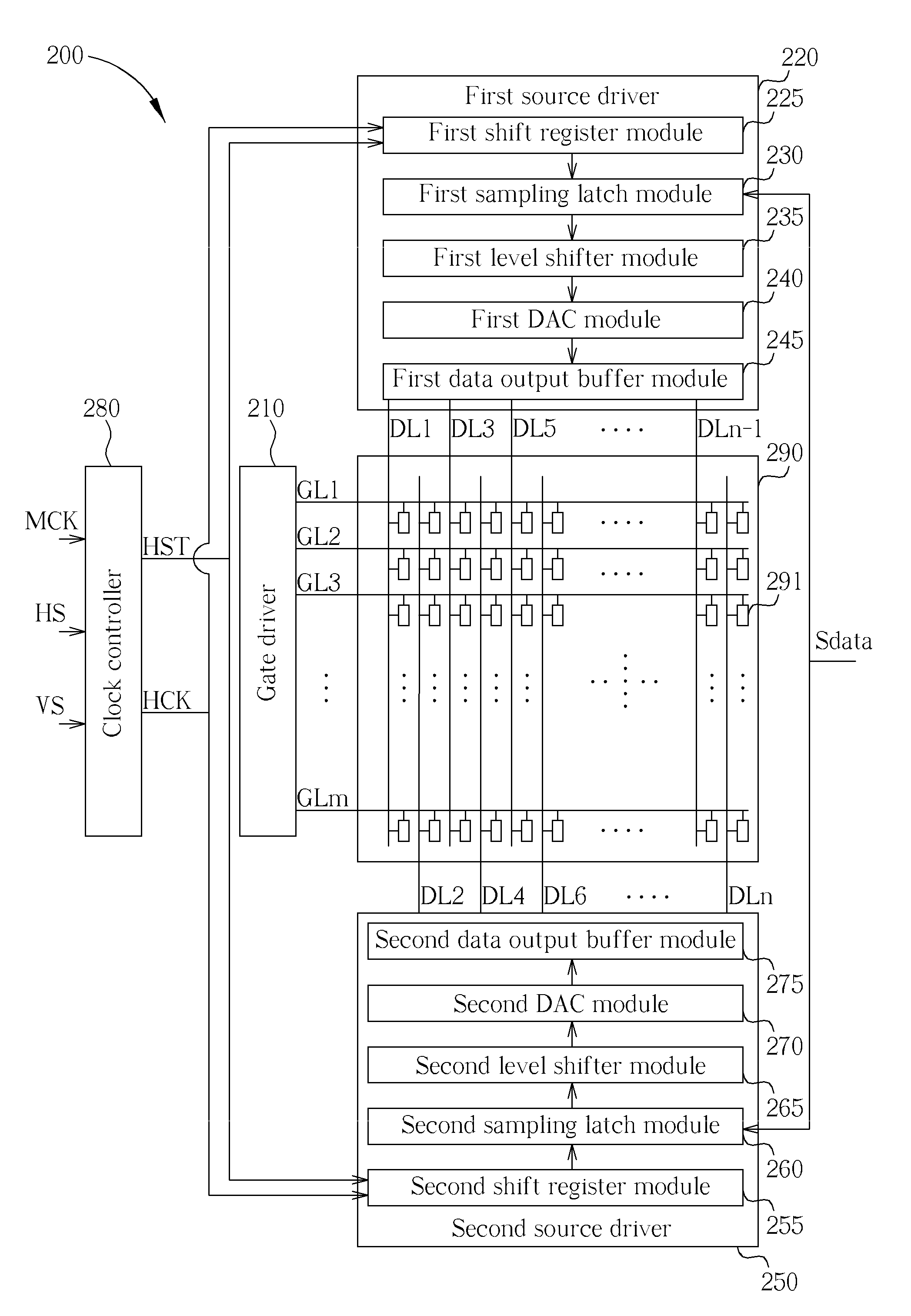
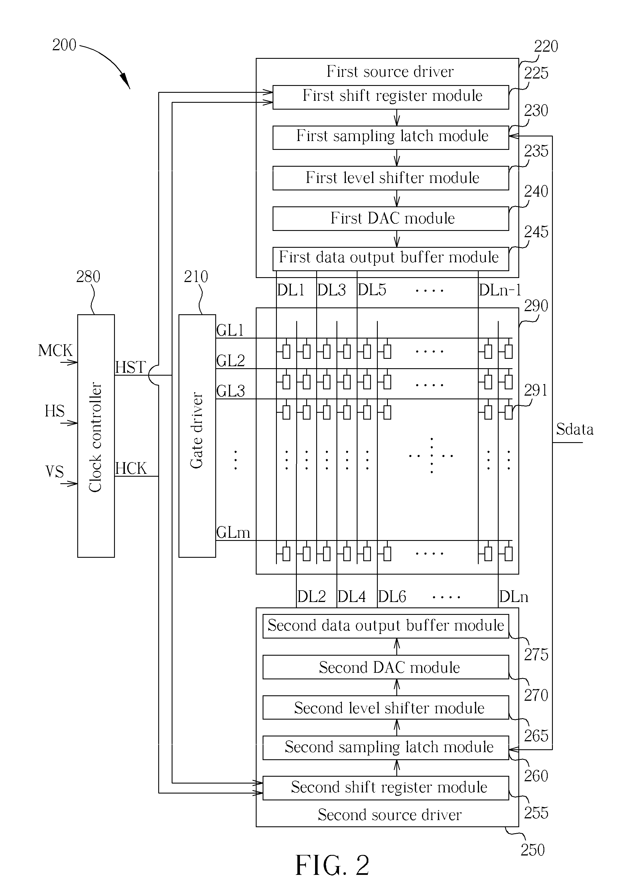
[0026]FIG. 2 is a schematic diagram showing an LCD device based on dual source drivers with data writing synchronous control mechanism in accordance with the present invention. As shown in FIG. 2, the LCD device 200 comprises a gate driver 210, a first source driver 220, a second source driver 250, a clock controller 280, an LCD panel 290, a plurality of gate lines GL1-GLm, and a plurality of data lines DL1-DLn. The clock controller 280 is utilized for generating a horizontal start signal HST and a horizontal clock signal HCK based on a master clock signal MCK, a horizontal synchronization signal HS, or a vertical synchronization signal VS. The first source driver 220 and the second source driver 250 are coupled to the clock controller 280 for receiving the horizontal start signal HST and the horizontal clock signal HCK. The LCD panel 290 comprises a plurality of pixel units 291. Each pixel unit 291 is coupled to a corresponding gate line and a corresponding data line.
[0027]The firs...
second embodiment
[0042]FIG. 6 is a schematic diagram showing an LCD device based on dual source drivers with data writing synchronous control mechanism in accordance with the present invention. As shown in FIG. 6, the LCD device 600 comprises a gate driver 610, a first source driver 620, a second source driver 650, a clock controller 680, an LCD panel 690, a plurality of gate lines GL1-GLm, and a plurality of data lines DL1-DLn. The clock controller 680 is utilized for generating a first horizontal start signal HST1, a first horizontal clock signal HCK1, a second horizontal start signal HST2, and a second horizontal clock signal HCK2 based on a master clock signal MCK, a horizontal synchronization signal HS, or a vertical synchronization signal VS. The first source driver 620 is coupled to the first and second output ends of the clock controller 680 for receiving the first horizontal start signal HST1 and the first horizontal clock signal HCK1 respectively. The second source driver 650 is coupled to...
PUM
 Abstract
Description
Claims
Application Information


