Techniques for arranging solder balls and forming bumps

a technology of solder balls and bumps, applied in the field of electrical and electronic arts, can solve the problems of inability to apply screen printing methods for fine pitch, inability to handle wide alloy range of electroplating methods, and inability to apply electric current induced composition control to fine pitch,

Inactive Publication Date: 2009-11-19
ULTRATECH INT INC
View PDF20 Cites 16 Cited by
  • Summary
  • Abstract
  • Description
  • Claims
  • Application Information

AI Technical Summary

Benefits of technology

[0014]In another aspect, another exemplary method includes providing a mold having a plurality of cavities; and dispensing conductive balls into the cavities, substantially one ball to each cavity, by tipping and vibrating the mold. The cavities in the mold are configured a

Problems solved by technology

As smaller solder bump interconnects, at finer pitch, are in great demand for flip chip technology, the ball drop method and C4NP, which eliminate the volume reduction problem, and which have solder alloy flexibility, have recently gained visibility and attention in the industry Around 50% volume reduction between solder pastes and final solder bumps after reflow makes it difficult to apply the screen printing method for fine pitch applications The electric current induced composition control can not handle wide alloy range in electrop

Method used


Image

  • Techniques for arranging solder balls and forming bumps
  • Techniques for arranging solder balls and forming bumps
  • Techniques for arranging solder balls and forming bumps

Examples


Embodiment Construction

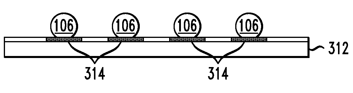
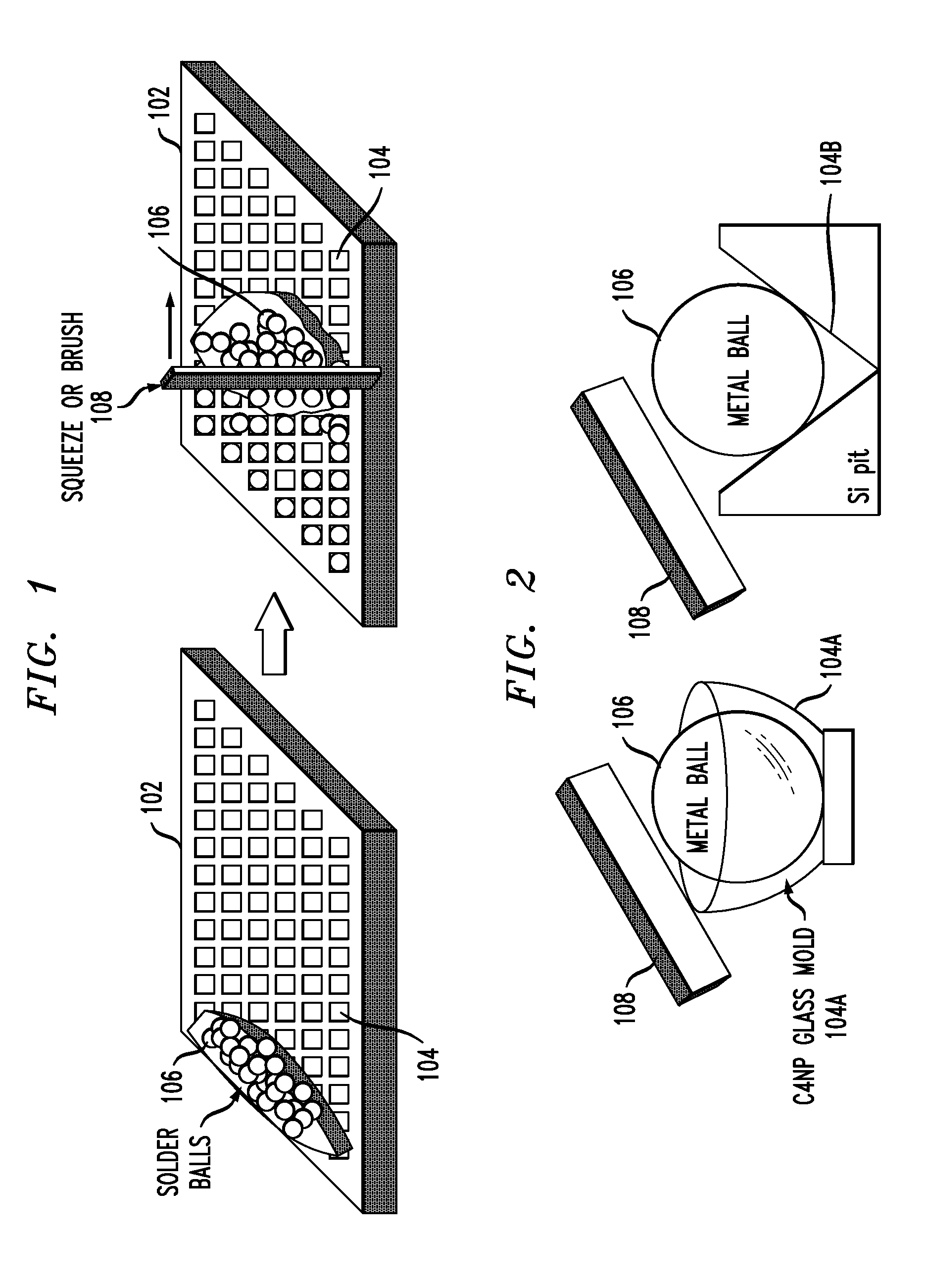
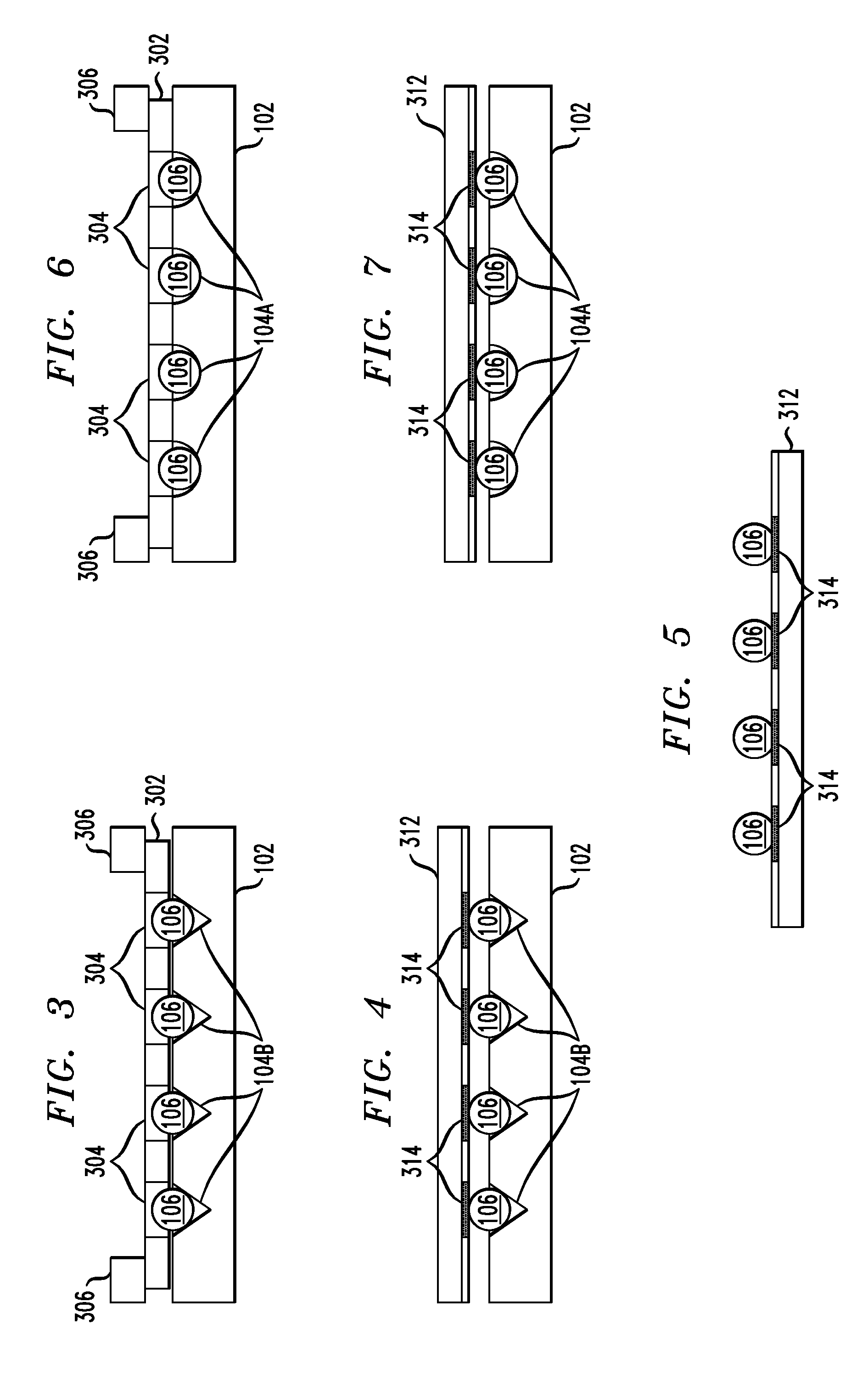
[0025]Current C4NP techniques require injection of molten solder. As noted, application of such techniques is limited for high-temperature cases, due to inability to find a suitable seal material. Aspects of the invention provide a method for arraying high melting temperature solder balls and forming solder bumps on a semiconductor device. The direct array of solder balls in the cavities of a mold plate, according to one or more embodiments of the invention, does not require any sealing materials (as in IMS). Accordingly, aspects of the invention provide techniques for placing high melting temperature solder balls into a C4NP mold plate to carry out a fluxless solder joining method.

[0026]With reference to FIGS. 1 and 2, a current C4NP mold plate 102 could be directly used for the array of solder balls 106; however, to make good contact between the solder balls 106 and the input / output (I / O) pads on a semiconductor device after the array of solder balls is formed, the top surface of ...


PUM

PropertyMeasurementUnit
Fractionaaaaaaaaaa
Fractionaaaaaaaaaa
Fractionaaaaaaaaaa

Abstract

A mask having a plurality of through holes and a mold having a plurality of cavities are provided, and the through holes and the cavities are aligned. Conductive balls ale dispensed into the aligned through holes and cavities Substantially one ball is dispensed into each aligned through hole and cavity, and the mask with the holes and the cavities in the mold ale configured and dimensioned such that the balls are substantially flush with, or recessed below, an outer surface of the mask. The mask is removed, the conductive balls are aligned with pads of a semiconductor device, and the conductive balls are transferred to the pads by fluxless reflow in a formic acid environment. Vibrational, electrostatic, and direct transfer aspects are also disclosed.

Description

FIELD OF THE INVENTION[0001]The present invention generally relates to the electrical and electronic arts and, more particularly, to techniques for forming electrical interconnections.BACKGROUND OF THE INVENTION[0002]There are many techniques that can be used for the fine pitch solder bumping process for so-called “flip chip” technology, including, for example, evaporation, electroplating, screen printing, hall drop, C4NP (Controlled Collapse Chip Connection—New Process), and so on.[0003]As smaller solder bump interconnects, at finer pitch, are in great demand for flip chip technology, the ball drop method and C4NP, which eliminate the volume reduction problem, and which have solder alloy flexibility, have recently gained visibility and attention in the industry Around 50% volume reduction between solder pastes and final solder bumps after reflow makes it difficult to apply the screen printing method for fine pitch applications The electric current induced composition control can no...

Claims


Application Information

Patent Timeline
IPC IPC(8): B23K1/20
CPCB23K1/0016B23K3/0623H01L2924/0001H01L2224/13111H01L2924/014H01L2924/01076H01L2924/01033H01L2924/01006H01L2924/01005H01L2224/11334H01L2224/11005H05K2203/105H05K2203/0557H05K2203/041H05K2203/0338H05K2203/0292H05K2203/0113H05K3/3478H01L2924/3025H01L2924/14H01L2924/09701H01L2924/01327H01L2924/01082H01L2924/01079H01L2924/01051B23K3/087B23K2201/40B23K2201/42H01L21/4853H01L21/6835H01L24/11H01L24/13H01L2224/11003H01L2224/13099H01L2924/01013H01L2924/01029H01L2924/0103H01L2924/01047H01L2924/00014B23K2101/40B23K2101/42H01L2224/05571H01L2224/05573H01L2224/06131H01L2924/181H01L2924/00H01L2224/05599
Inventor BUDD, RUSSELL A.LIBSCH, FRANK R.NAH, JAE-WOONG
Owner ULTRATECH INT INC
Why Eureka
Try Eureka