Ion Implanter For Photovoltaic Cell Fabrication

a photovoltaic cell and implanter technology, applied in nuclear engineering, separation processes, mass spectrometry, etc., can solve the problems of wasting a substantial amount of silicon, unable to optimize the way of forming crystalline silicon bodies for photovoltaic cells, and affecting the efficiency of photovoltaic cells,

Inactive Publication Date: 2009-11-19
NEUTRON THERAPEUTICS LLC
View PDF12 Cites 13 Cited by
  • Summary
  • Abstract
  • Description
  • Claims
  • Application Information

AI Technical Summary

Benefits of technology

[0014]In another embodiment, the invention provides a method of making a photovoltaic device, comprising providing a semiconductor wafer; providing a first appliance configured to hold the wafer; providing a first ion train including a first ion source configured to generate hydrogen or helium ions, a first mass analyzer, having a resolving power less than ten, configured to sort ions from the first ion source according to their respective mass / charge ratios and further configured to direct selected ions toward the first appliance in an ion beam, and a first voltage apparatus configured to apply a first voltage drop between the first ion source and the first appliance; installing the semiconductor wafer in the first appliance; operating the first ion train to generate, select, and accelerate ions of a first species toward the first appliance in a first ion beam, thereby implanting the ions of the first species in the wafer at a depth defining a cleave plane; annealing the wafer to effect cleaving of a lamina from the wafer at the cleave plane, the lamina being at least 1μm thick; and fabricating the photovoltaic device from the lamina. Illustratively, the first ion train has no other mass analyzer besides the first mass analyzer. The selected ions of the first species may constitute a first current of at least 5 mA in the first ion beam, and the first species is illustratively hydrogen or helium.

Problems solved by technology

Nevertheless, a way of forming crystalline silicon bodies optimized for photovoltaic cells has remained elusive.
This process, which typically yields a silicon wafer thicker than 150 μm, wastes a substantial amount of silicon by consuming up to 50% of the silicon body in kerf loss and delivering a much greater thickness than is needed for useful photovoltaic devices.
The films produced this way have found application in forming silicon-on-insulator structures but are cost-prohibitive for solar cells.
Also, at thicknesses well under 1 μm, the films may be so thin as to make efficient light-capturing difficult.
Boosting the energy of ion implant could increase the film thickness, but this adaptation would make the films even more expensive and less economical for photovoltaics.

Method used


Image

  • Ion Implanter For Photovoltaic Cell Fabrication
  • Ion Implanter For Photovoltaic Cell Fabrication
  • Ion Implanter For Photovoltaic Cell Fabrication

Examples


Embodiment Construction

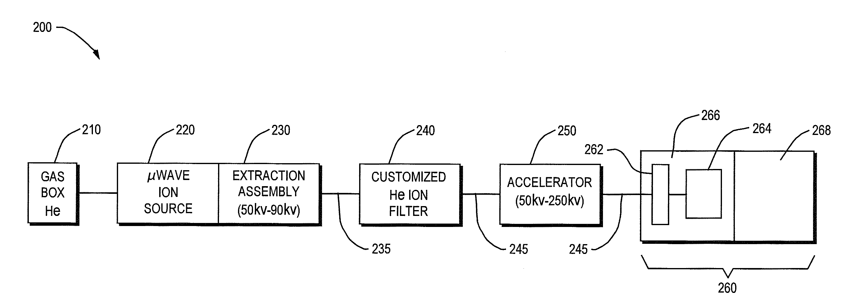
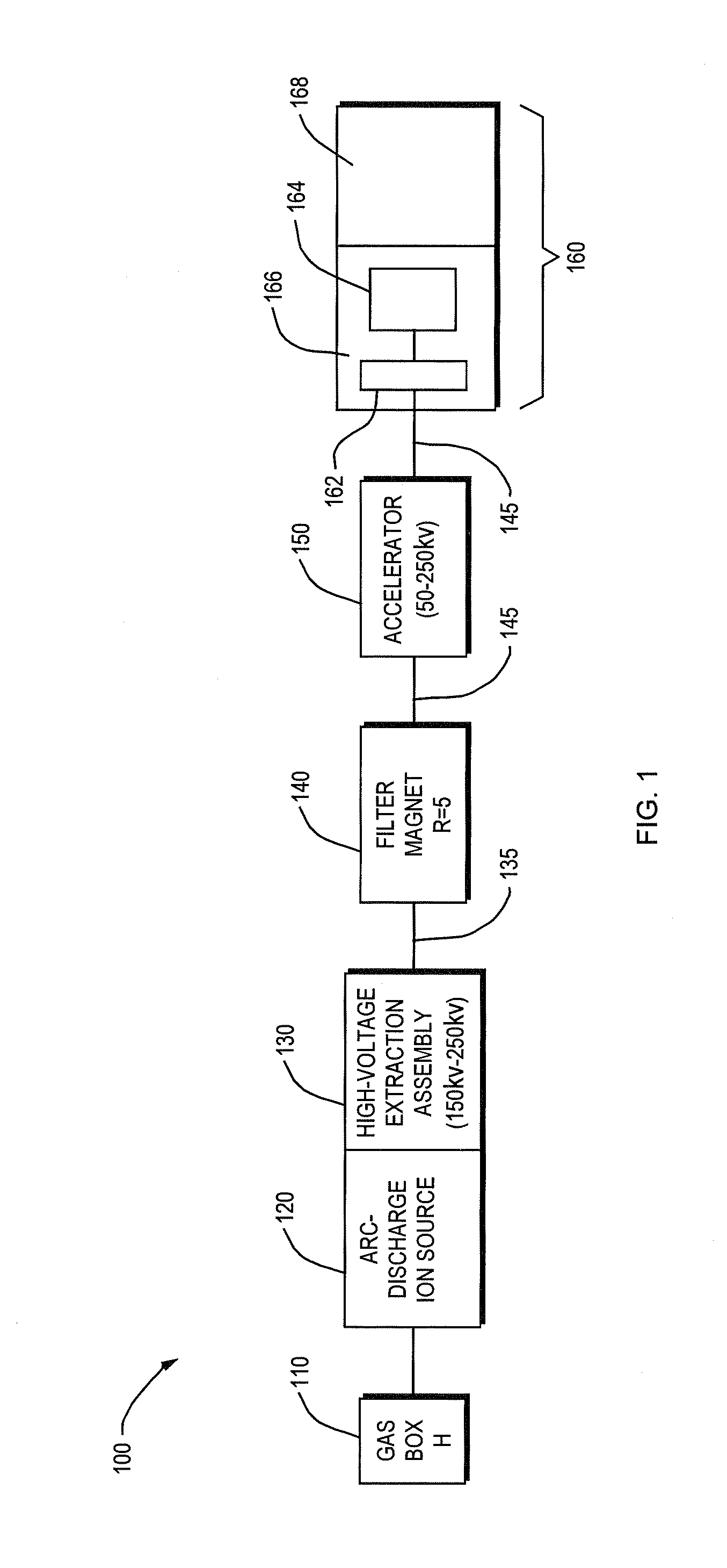
[0023]The invention relates to ion implanters useful for economically implanting semiconductor wafers preparatory to photovoltaic cell fabrication. Techniques for making semiconductor laminae for photovoltaic applications by cleaving after high-dose implantation of hydrogen or helium are described in co-owned U.S. application Ser. No. 12 / 057,265, Sivaram et al., “Method to Form a Photovoltaic Cell Comprising a Thin Lamina,” the disclosure of which is incorporated herein by reference. Hydrogen, helium, or both are implanted in a wafer of semiconductor material, such as monocrystalline silicon, at a depth defining a cleave plane, which determines a lamina thickness. Removal of the lamina from the implanted wafer is effected by, for example, annealing the wafer to provoke exfoliation of the lamina at the cleave plane.

[0024]For preparation of efficient photovoltaic devices, lamina thicknesses of about 1 micron and greater are desirable. The location of the cleave plane is related to the...


PUM


Abstract

Ion implanters are especially suited to meet process dose and energy demands associated with fabricating photovoltaic devices by ion implantation followed by cleaving.

Description

BACKGROUND OF THE INVENTION[0001]1. Field of the Invention[0002]This invention relates to ion implanters for preparing semiconductor lamina, and, in particular, ion implanters used for economical production of photovoltaic cells.[0003]2. Background Information[0004]As the demand for electrical energy based on renewable sources increases, the implementation of photovoltaic technology has expanded dramatically in recent years. Nevertheless, a way of forming crystalline silicon bodies optimized for photovoltaic cells has remained elusive.[0005]Crystalline silicon wafers adapted to bear photovoltaic cells are conventionally obtained by slicing a silicon ingot. This process, which typically yields a silicon wafer thicker than 150 μm, wastes a substantial amount of silicon by consuming up to 50% of the silicon body in kerf loss and delivering a much greater thickness than is needed for useful photovoltaic devices.[0006]Thinner silicon laminae have been made by exfoliation of a film by ann...

Claims


Application Information

Patent Timeline
Patent Type & Authority Applications(United States)
IPC IPC(8): H01J49/26G21K5/10
CPCH01J37/05H01J2237/2007H01J37/3171H01J37/20
Inventor PARRILL, THOMASAGARWAL, ADITYA
Owner NEUTRON THERAPEUTICS LLC
Why Eureka
Try Eureka