Nonvolatile memory element, manufacturing method thereof, and nonvolatile semiconductor apparatus using the nonvolatile memory element

Active Publication Date: 2009-11-19
PANASONIC SEMICON SOLUTIONS CO LTD
View PDF4 Cites 184 Cited by
  • Summary
  • Abstract
  • Description
  • Claims
  • Application Information

AI Technical Summary

Benefits of technology

[0047]According to the present invention, it is possible to attain a nonvolatile memory element which is capable of performing a high-speed operation and has reversibly-stable rewrite characteristics and desirable resistance value retention characteri

Problems solved by technology

It is said that, in response to these demands, miniaturization of

Method used


Image

  • Nonvolatile memory element, manufacturing method thereof, and nonvolatile semiconductor apparatus using the nonvolatile memory element
  • Nonvolatile memory element, manufacturing method thereof, and nonvolatile semiconductor apparatus using the nonvolatile memory element
  • Nonvolatile memory element, manufacturing method thereof, and nonvolatile semiconductor apparatus using the nonvolatile memory element

Examples


embodiment 1

[Configuration of Nonvolatile Memory Element]

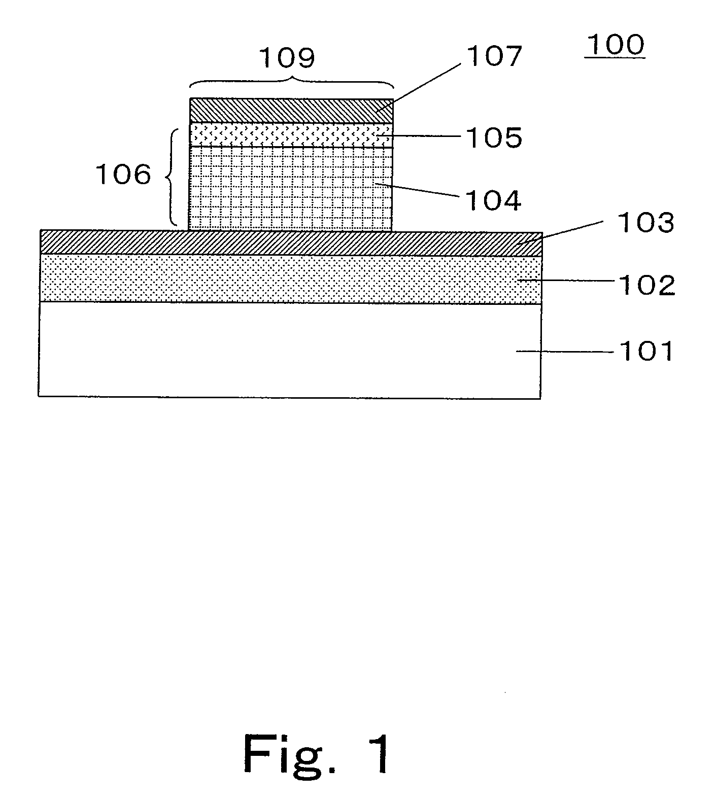
[0150]FIG. 1 is a cross-sectional view showing an example of a configuration of a nonvolatile memory element according to Embodiment 1 of the present invention.

[0151]As shown in FIG. 1, a nonvolatile memory element 100 of this embodiment comprises a substrate 101, an oxide layer 102 formed on the substrate 101, a first electrode layer 103 formed on the oxide layer 102, a second electrode layer 107, and a resistance variable layer 106 sandwiched between the first electrode layer 103 and the second electrode layer 107. The resistance variable layer 106 comprises an oxygen-deficient tantalum oxide having a composition represented by TaOz (0106 comprises a first tantalum-containing layer (first region: hereinafter referred to as “first tantalum oxide layer”) 104 having a low oxygen content rate, and a second tantalum-containing layer (second region: hereinafter referred to as “second tantalum oxide layer) 105 formed on the first tantalum oxid...

embodiment 2

[0219]In Embodiment 1, after the first tantalum oxide layer was deposited inside the sputtering apparatus, oxidation treatment using oxygen plasma was subsequently performed to form the second tantalum oxide layer. In this method, however, a thick second tantalum oxide layer was not be able to be formed because of the used apparatus. Therefore, in Embodiment 2, the operation of a nonvolatile memory element having a thick second tantalum oxide layer will be described.

[Method of Manufacturing Nonvolatile Memory Element]

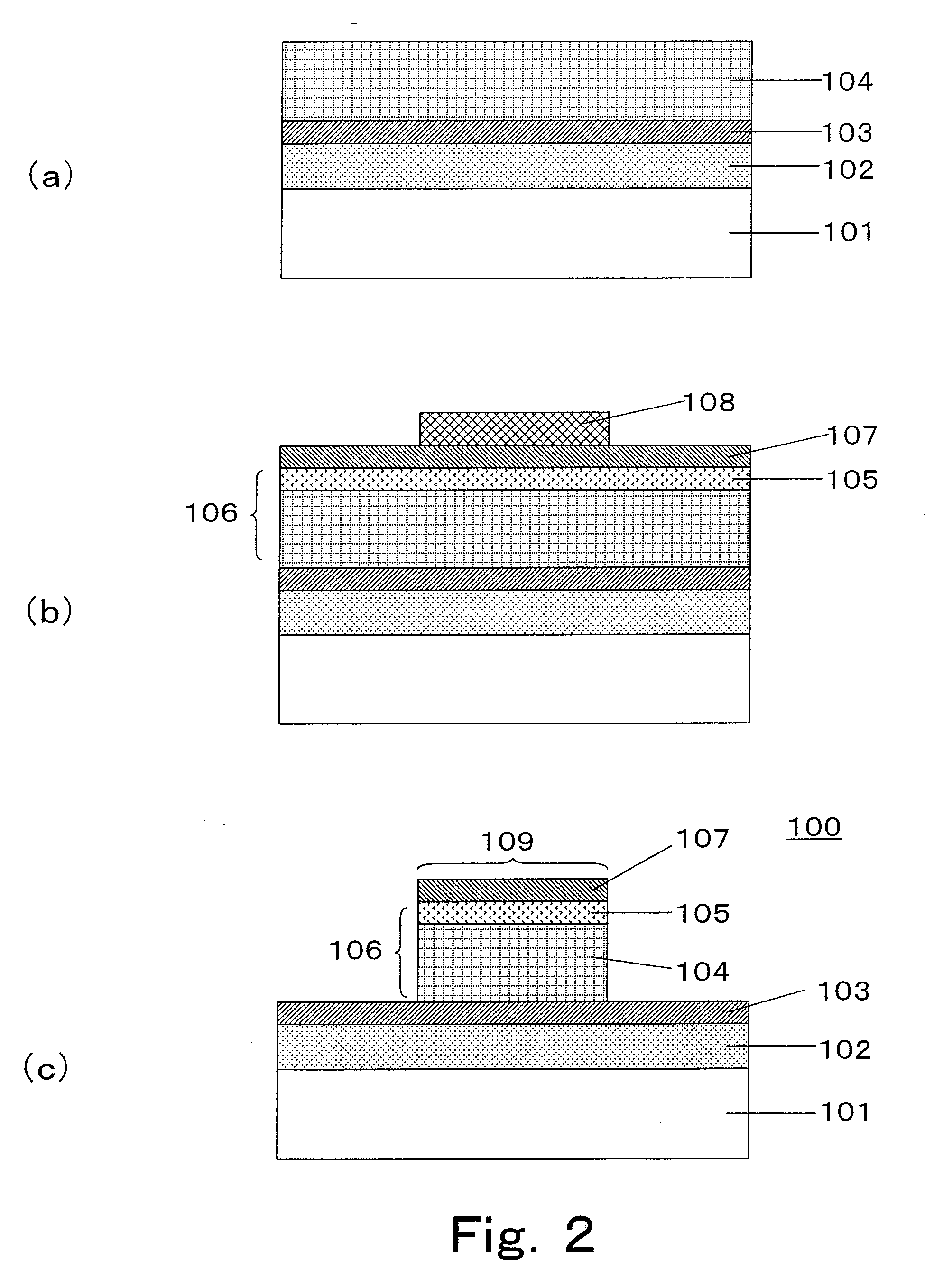
[0220]The method of manufacturing the nonvolatile memory element is fundamentally identical to that of Embodiment 1. However, for the convenience of the oxidation process, the deposition condition of the tantalum oxide and the size of the manufactured nonvolatile memory element are different from those of Embodiment 1. Hereinafter, the process of manufacturing the nonvolatile memory element will be described with reference to FIG. 2.

[0221]Initially, as shown in FIG. 2(a...

embodiment 3

[0237]In the above described nonvolatile memory element 100 according to Embodiment 1, the oxygen content rate of the first tantalum oxide layer 104 was 58 at % (TaO1.4). The oxygen content rate of the first tantalum oxide layer 104 in the nonvolatile memory element 100 according to Embodiment 2 was close to that of Embodiment 1, i.e., 61 at % (TaO1.6). In contrast, a nonvolatile memory element according to Embodiment 3 includes a first tantalum oxide layer whose oxygen content rate is varied in a little larger range. Since the other constituents of Embodiment 3 are identical to those of Examples 1 and 2, illustration thereof will be omitted. Hereinafter, a description will be made of the manufacturing methods and the resistance varying characteristics of Examples in this embodiment which are manufactured in such a way that the oxygen content rate of the first tantalum oxide layer is changed, with reference to FIG. 1.

[Relation Between Oxygen Flow Rate Ratio During Sputtering and Com...


PUM


Abstract

A nonvolatile memory element comprises a first electrode layer (103), a second electrode (107), and a resistance variable layer (106) which is disposed between the first electrode layer (103) and the second electrode layer (107), a resistance value of the resistance variable layer varying reversibly according to electric signals having different polarities which are applied between the electrodes (103), (107), wherein the resistance variable layer (106) has a first region comprising a first oxygen-deficient tantalum oxide having a composition represented by TaOx (0<x<2.5) and a second region comprising a second oxygen-deficient tantalum oxide having a composition represented by TaOy (x<y<2.5), the first region and the second region being arranged in a thickness direction of the resistance variable layer.

Description

TECHNICAL FIELD[0001]The present invention relates to a nonvolatile memory element. More particularly, the present invention relates to a resistance variable nonvolatile memory element whose resistance value varies according to an applied electric signal, a manufacturing method thereof, and a nonvolatile semiconductor apparatus using the nonvolatile memory element.BACKGROUND ART[0002]In recent years, with the advancement of digital technologies, higher functionality of electronic hardware such as portable information devices and information appliances have been provided. Therefore, demands for an increase in a capacity of a nonvolatile memory element, reduction in a writing power in the memory element, reduction in write / readout time of the memory element, and longer life of the memory element have been increasing.[0003]It is said that, in response to these demands, miniaturization of an existing flash memory using a floating gate has a limitation. Accordingly, a novel resistance va...

Claims


Application Information

Patent Timeline
IPC IPC(8): H01L45/00H01L21/16H01L29/12
CPCG11C13/0007G11C2013/0073G11C2213/71G11C2213/72G11C2213/79H01L27/101H01L45/08H01L45/1233H01L45/146H01L45/1625H01L45/1675H01L27/2409H01L27/2436H01L27/2481Y10S438/90G11C13/004G11C13/0069G11C2213/32H10B63/84H10B63/20H10B63/30H10N70/24H10N70/026H10N70/8833H10N70/063H10N70/826H10N70/231
Inventor KANZAWA, YOSHIHIKOKATAYAMA, KOJIFUJII, SATORUMURAOKA, SHUNSAKUOSANO, KOICHIMITANI, SATORUMIYANAGA, RYOKOTAKAGI, TAKESHISHIMAKAWA, KAZUHLKO
Owner PANASONIC SEMICON SOLUTIONS CO LTD
Why Eureka
Try Eureka