Electromagnetic wave absorber using resistive material

a technology of resistive material and electromagnetic wave absorber, which is applied in the direction of electrical equipment, magnetic/electric field screening, and antennas, etc., can solve the problems of lowering eyesight, leukemia, brain tumor, and influence of electromagnetic waves generated from terminals on human body, etc., and achieves easy adjustment of absorbing frequency band and absorbing characteristics, simple manufacturing process, and easy adjustment of thickness

Inactive Publication Date: 2009-11-19
ELECTRONICS & TELECOMM RES INST
View PDF23 Cites 29 Cited by
  • Summary
  • Abstract
  • Description
  • Claims
  • Application Information

AI Technical Summary

Benefits of technology

[0008]Therefore, the present invention has been made in view of the above problems, and it is an object of the present invention to provide an electromagnetic wave absorber made of a resistive material using an Electromagnetic BandGap (EBG) structure, which has a simple manufacturing process, and easily adjusts an absorbing frequency band and absorbing characteristics by adjusting parameters, and has an adjustable thickness.

Problems solved by technology

However, as portable instruments have been increasingly used, the influence of electromagnetic waves generated from the terminals on the human body becomes an important issue.
The influence of electromagnetic waves at a frequency band used by portable terminals on the human body is not clearly known now, but it has been reported that the electromagnetic waves may cause leukemia, a brain tumor, a headache, a lowering of eyesight, and confusion of brain waves, destruction of men's reproductive function, and various diseases, when they are accumulated in the human body.
These electromagnetic wave absorbers are developed by a trial and error method, and thus have a complicated manufacturing process and cause a difficulty in adjusting an absorbing frequency band and absorbing characteristics.
However, these resonant absorbers are disadvantageous in that the thickness of the dielectric spacer from the metal conductive ground surface is at least λ / 4.

Method used


Image

  • Electromagnetic wave absorber using resistive material
  • Electromagnetic wave absorber using resistive material
  • Electromagnetic wave absorber using resistive material

Examples


Embodiment Construction

[0029]Now, preferred embodiments of the present invention will be described in detail with reference to the annexed drawings.

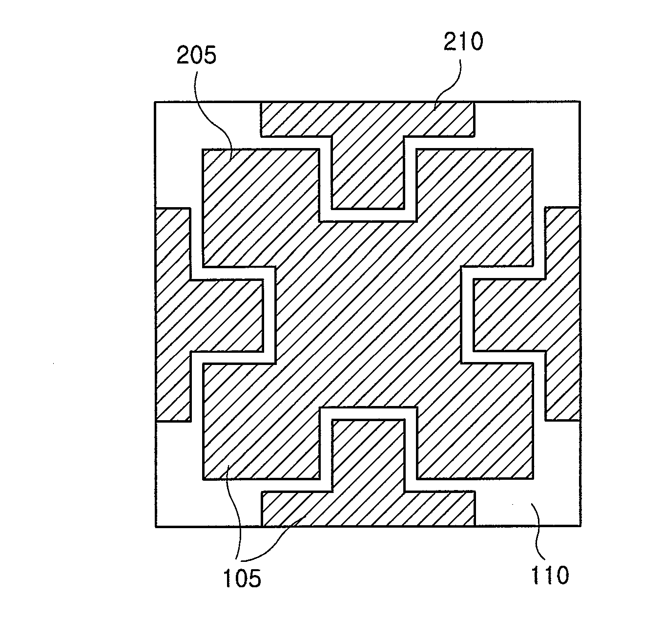
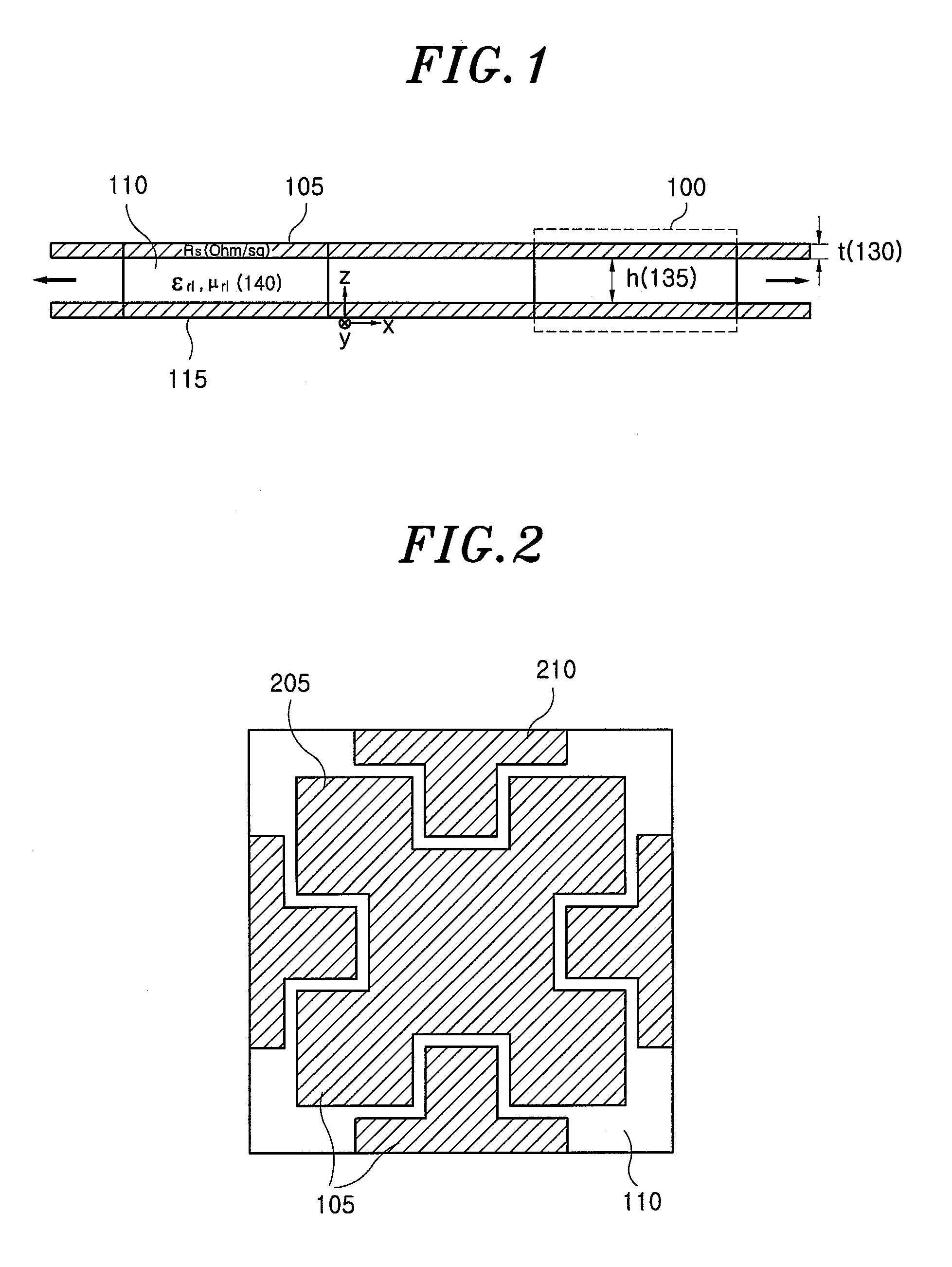
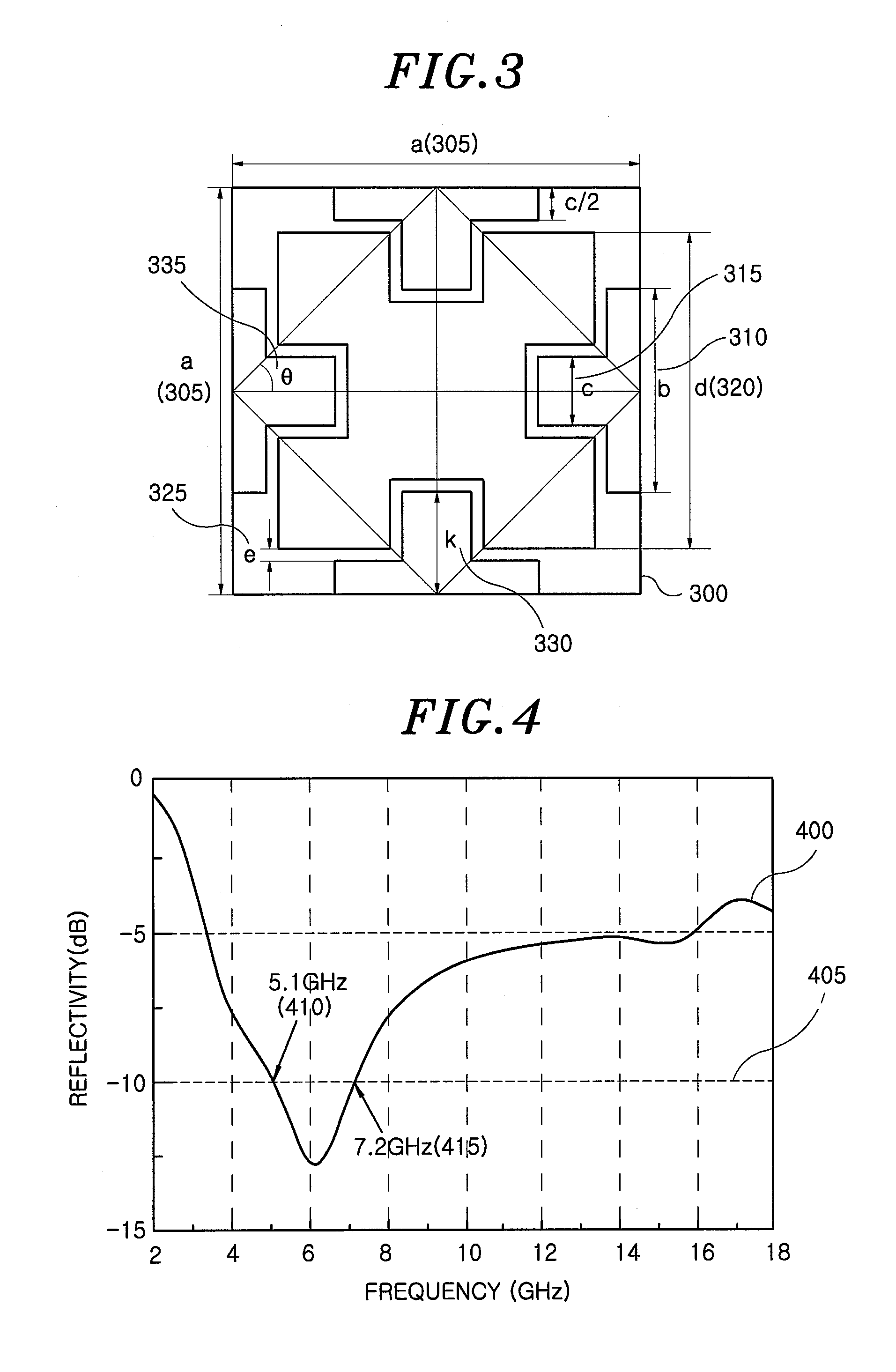
[0030]FIG. 1 is a front view of one embodiment of an electromagnetic wave absorber using a resistive material in accordance with the present invention. With reference to FIG. 1, an electromagnetic wave absorber is obtained by periodically arranging unit cells 100 of an Electromagnetic BandGap (EBG), each of which includes a metal conductive ground surface 115, a dielectric layer 110 formed on the metal conductive ground surface 115, and a unit cell pattern 105 made of a resistive material and formed on the dielectric layer 110.

[0031]The dielectric layer 110 and the unit cell pattern 105 made of the resistive material form a structure adding a loss to a frequency selective surface (FSS), and thus serve to partially reflect and partially transmit incident waves at a desired frequency and to adjust phases of the waves in the dielectric layer 110. Further, the met...


PUM


Abstract

An electromagnetic wave absorber includes a ground layer made of a metal conductor, a dielectric layer formed on the ground layer, and a unit cell pattern made of a resistive material, and formed on the dielectric layer. The unit cell pattern includes a fundamental patch having a regular square shape, in which a rectangular recess is formed on the center of each of the respective sides, the fundamental patch being located at the center of each of the unit cell pattern, and half cross dipole patches, which are respectively disposed at the four sides of the fundamental patch at a regular angle so as to be engaged with the recesses formed on the respective sides of the fundamental patch at a regular interval.

Description

CROSS-REFERENCE(S) TO RELATED APPLICATIONS[0001]The present invention claims priority of Korean Patent Application No. 10-2008-0044515, filed on May 14, 2008, which is incorporated herein by reference.FIELD OF THE INVENTION[0002]The present invention relates to a resonant electromagnetic wave absorber using a resistive material, and more particularly to an electromagnetic wave absorber made of a resistive material, in which the whole pattern, obtained by periodically arranging unit cells, properly adjusts the phases of reflected waves and transmitted waves using an Electromagnetic BandGap (EBG) structure so as to absorb electromagnetic waves.[0003]This work was supported by the IT R&D program of MIC / IITA[2007-F-043-01, Study on Diagnosis and Protection Technology based on EM]BACKGROUND OF THE INVENTION[0004]As information technology (IT) has been rapidly developed and a desire for Internet communication has been increased, wireless communication instruments including a portable term...

Claims


Application Information

Patent Timeline
Patent Type & Authority Applications(United States)
IPC IPC(8): H01Q17/00
CPCH01Q17/00H05K9/00
Inventor SIM, DONG-UKKWON, JONG HWAKWAK, SANG ILCHOI, HYUNG DO
Owner ELECTRONICS & TELECOMM RES INST
Why Eureka
Try Eureka