Testing a memory device having field effect transistors subject to threshold voltage shifts caused by bias temperature instability

a technology of field effect transistor and threshold voltage, which is applied in the field of field effect transistor (fet) circuits, can solve the problems of pfet threshold voltage shift, sram is usually faster, more expensive than dram, and sram and dram are typically volatil

Inactive Publication Date: 2009-11-19
QUALCOMM INC
View PDF8 Cites 21 Cited by
  • Summary
  • Abstract
  • Description
  • Claims
  • Application Information

AI Technical Summary

Benefits of technology

[0019]According to one aspect of the present invention, a supply voltage is set for the memory device at a first supply voltage level. Test data is written to the memory device at the first supply voltage level in response to setting the supply voltage. The supply voltage is decreased for the memory device to a second supply voltage level below the first supply voltage level in response to writing the test data. The test data is read from the memory device at the second supply voltage level in response to decreasing the supply voltage. The

Problems solved by technology

SRAM is usually faster, but more expensive than DRAM.
Both SRAM and DRAM are typically volatile in the sense that they lose data when power is removed from the memory chip.
Due to the reduced physical sizes and the reduction in threshold voltages (VT) of the FETs, threshold voltage (VT) shifts in PFETs caused by negative bias temperature instability (NBTI) are becoming a significant reliability issue.
Therefore, threshold voltage (VT) shift in PFETs caused by NBTI is a significant threat to SRAM reliability.
NBTI also causes what might have been marginal, but operative, memory storage locations to become failing storage locations, such as degrading the READ stabi

Method used


Image

  • Testing a memory device having field effect transistors subject to threshold voltage shifts caused by bias temperature instability
  • Testing a memory device having field effect transistors subject to threshold voltage shifts caused by bias temperature instability
  • Testing a memory device having field effect transistors subject to threshold voltage shifts caused by bias temperature instability

Examples


Embodiment Construction

[0027]The following description and drawings are illustrative of the invention and are not to be construed as limiting the invention. Numerous specific details are described to provide a thorough understanding of the present invention. However, in certain instances, well-known or conventional details are not described in order to avoid obscuring the description of the present invention. References to one embodiment or an embodiment in the present disclosure are not necessarily to the same embodiment, and such references include one or more embodiments.

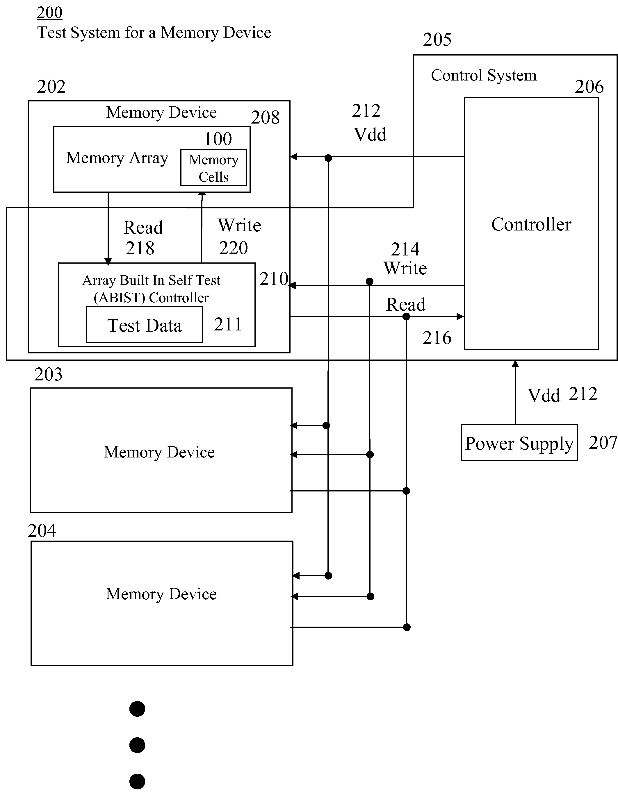
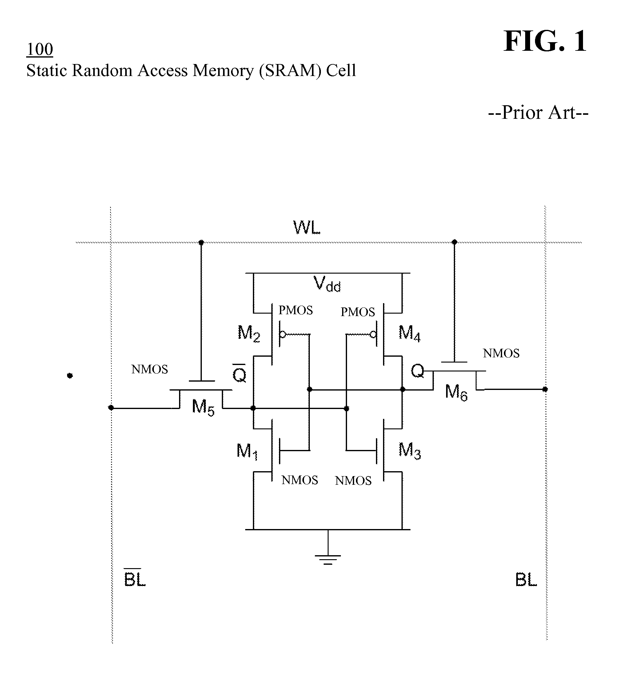
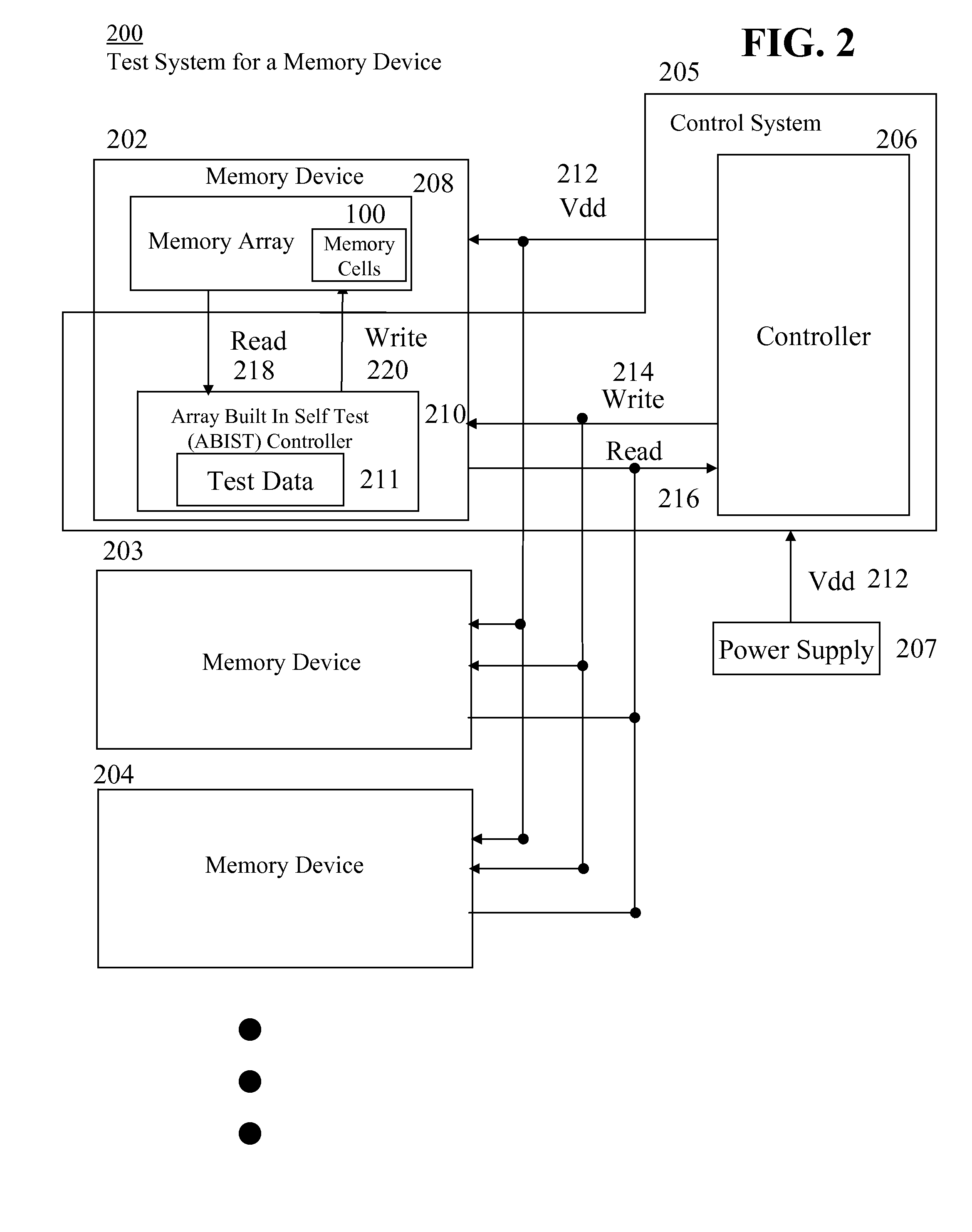
[0028]FIG. 1 illustrates static random access memory (SRAM) cell 100 having field effect transistors subject to threshold voltage shifts caused by bias temperature instability, according to the prior art. The SRAM cell includes six transistors and incorporates CMOS technology. The six transistors (M1-M6) typically include four n-channel metal-oxide-semiconductor field effect transistors (NMOSFET) (M1, M3, M5, M6) and two p-channel MOSF...


PUM


Abstract

A supply voltage is set for a memory device at a first supply voltage level. Test data is written to the memory device at the first supply voltage level in response to setting the supply voltage. The supply voltage is decreased for the memory device to a second supply voltage level below the first supply voltage level in response to writing the test data. The test data is read from the memory device at the second supply voltage level in response to decreasing the supply voltage. The supply voltage is increased for the memory device to a third supply voltage level above the second supply voltage level in response to reading the test data. The test data is read from the memory device at the third supply voltage level in response to increasing the supply voltage. The test data written to the memory device at the first supply voltage level is compared to the test data read from the memory device at the third supply voltage level in response to reading the test data from the memory device at the third supply voltage level.

Description

FIELD OF THE INVENTION[0001]The present invention generally relates to field effect transistor (FET) circuits. More specifically, the present invention relates to testing a memory device having field effect transistors (FET) subject to threshold voltage (VT) shifts caused by bias temperature instability (BTI).BACKGROUND OF THE INVENTION[0002]Modern electronic devices and systems, for example, computer processors, mobile telephones, personal digital assistants (PDAs), digital cameras, and combinations thereof currently rely on logic (e.g., controller) and storage (e.g., memory) circuits fabricated with semiconductor materials to form integrated circuits called chips.[0003]Random access memory (RAM) is an example of a common storage circuit that permits data to be accessed in any order (e.g., randomly), regardless of the data's physical location in the memory chip and regardless of whether or not the data is related to previous data. Two types of RAM include Static RAM (SRAM), which t...

Claims


Application Information

Patent Timeline
IPC IPC(8): F21V29/00
CPCG11C11/41G11C29/50G11C29/12005G11C29/10
Inventor CHEN, NANLEE, SIAN-YEE SEANJUNG, SEONG-OOKWANG, ZHONGZE
Owner QUALCOMM INC
Why Eureka
Try Eureka