Solar cell spin-on based process for simultaneous diffusion and passivation

a spin-on and solar cell technology, applied in the field of solar cells, can solve the problems of contaminating silicon wafers, increasing manufacturing costs, and increasing operations, and achieve the effect of increasing manufacturing costs and increasing the number of operations

Inactive Publication Date: 2009-11-19
GEORGIA TECH RES CORP
View PDF53 Cites 23 Cited by
  • Summary
  • Abstract
  • Description
  • Claims
  • Application Information

AI Technical Summary

Benefits of technology

[0011]The use of the back sacrificial masking layer and the use of two high temperature furnace operations increase the number of operations for fabricating a solar cell, and thus increase manufacturing costs. Moreover, a high quality rear surface passivation by silicon dioxide typically requires a growth of a thick silicon dioxide layer, which involves a high-temperature oxidation operation over a long period of time. This raises concerns of contaminants from the furnace contaminating the silicon wafer.

Problems solved by technology

The use of the back sacrificial masking layer and the use of two high temperature furnace operations increase the number of operations for fabricating a solar cell, and thus increase manufacturing costs.
Moreover, a high quality rear surface passivation by silicon dioxide typically requires a growth of a thick silicon dioxide layer, which involves a high-temperature oxidation operation over a long period of time.
This raises concerns of contaminants from the furnace contaminating the silicon wafer.

Method used


Image

  • Solar cell spin-on based process for simultaneous diffusion and passivation
  • Solar cell spin-on based process for simultaneous diffusion and passivation
  • Solar cell spin-on based process for simultaneous diffusion and passivation

Examples


Embodiment Construction

[0018]In the following detailed description, numerous specific details are set forth in order to provide a thorough understanding of the invention. However, it will be understood by those skilled in the art that the present invention may be practiced without these specific details. In other instances, well-known methods, procedures, components, and circuits have not been described in detail so as not to obscure the present invention.

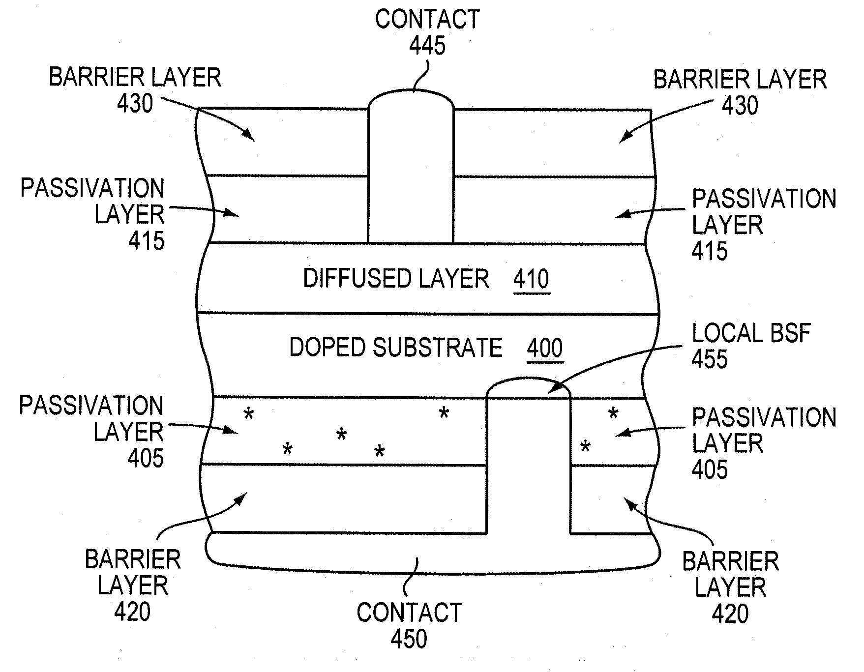
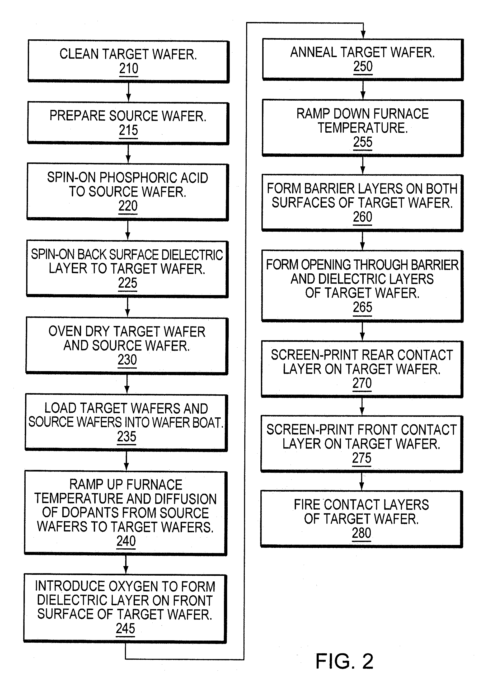
[0019]FIG. 2 is a flowchart for one embodiment of a process for creating simultaneous emitter diffusion and front and rear surface passivation. To minimize handling of cell wafers, this process involves a single diffusion and oxidation furnace operation. The process starts with silicon wafers, one of which is used as a dopant source wafer and the other of which is a target wafer on which the solar cell is to be formed. The target wafers may be Czochralski or Float Zone wafers. The target wafers may have a thickness from 50 to 500 micrometers. The target ...


PUM


Abstract

A thin silicon solar cell having a high quality spin-on dielectric layer is described. Specifically, the solar cell may be fabricated from a crystalline silicon wafer having a thickness from 50 to 500 micrometers. A first dielectric layer is applied to the rear surface of the silicon wafer using a spin-on process. A high temperature furnace operation provides simultaneous emitter diffusion and front and rear surface passivation. During this high temperature operation, the front emitter is formed, the rear spin-on dielectric layer is cured, and the front dielectric layer is thermally grown. Barrier layers are formed on the dielectric layers. Openings are made in the barrier layers. Contacts are formed in the openings and on the back surface barrier layer.

Description

GOVERNMENT INTERESTS[0001]The U.S. Government has a paid-up nonexclusive, nontransferable, worldwide license in this invention and the right in limited circumstances to require the patent owner to license others on reasonable terms as provided for by the terms of contract No. DE-FC36-07GO17023 awarded by the U.S. Department of Energy.FIELD OF THE INVENTION[0002]The present invention generally relates to silicon solar cells. More particularly, the present invention relates to a spin-on process for simultaneous emitter diffusion and passivation on a back surface of the solar cell.BACKGROUND OF THE INVENTION[0003]Solar cells are devices that convert light energy into electrical energy. These devices are also often called photovoltaic (PV) cells. Solar cells are manufactured from a wide variety of semiconductors. One common semiconductor material is crystalline silicon.[0004]Solar cells have three main elements: (1) a semiconductor; (2) a semiconductor junction; and (3) conductive conta...

Claims


Application Information

Patent Timeline
Patent Type & Authority Applications(United States)
IPC IPC(8): H01L31/18H01L21/02
CPCH01L31/02167Y02E10/547H01L31/1868H01L31/1804Y02P70/50
Inventor ROHATGI, AJEETMEEMONGKOLKIAT, VICHAIRAMANATHAN, SAPTHARISHI
Owner GEORGIA TECH RES CORP
Why Eureka
Try Eureka