
Compound Material for Inorganic Phosphor and White LED

a technology of inorganic phosphor and compound materials, which is applied in the direction of luminescent compositions, semiconductor devices, chemistry apparatuses and processes, etc., can solve the problems of reducing the luminous efficiency of led, not being used for useful applications, and increasing the temperature inside the heterostructure, so as to eliminate the drawbacks of conventional led optical performan

Inactive Publication Date: 2009-11-26
LO WEI HUNG
View PDF1 Cites 14 Cited by
  • Summary
  • Abstract
  • Description
  • Claims
  • Application Information

AI Technical Summary

Benefits of technology

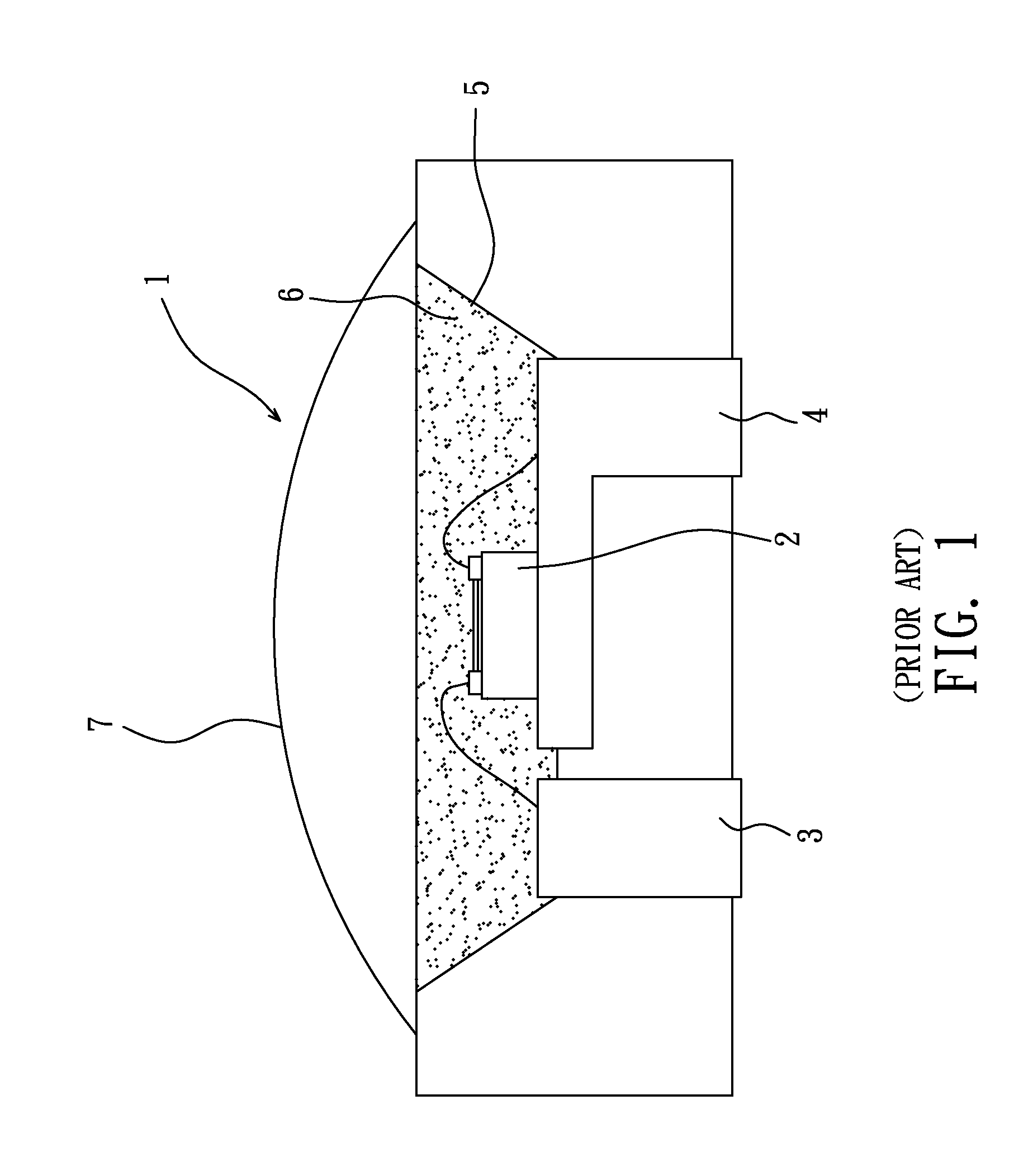
[0014]The present invention has been accomplished under the circumstances in view. It is therefore the main object of the present invention to provide a compound material for LED, which uses dispersed inorganic dispersant powder, eliminating conventional LED optical drawbacks.
[0015]It is another object of the present invention to provide a compound material for LED, which has a supplementary composition added to the phosphor conversion layer, lowering first order radiation and total radiation losses.
[0016]It is still another object of the present invention to provide a compound material for LED, which corrects the total radiation of the LED, providing a warm color tone.
[0017]It is still another object of the present invention to provide a compound material for LED, which improves the luminous intensity of the LED.

Problems solved by technology

These discoveries were not employed for useful application at the time they were firstly disclosed or 15 years after their disclosure.
However, LED market monopoly by Japanese manufacturers imparts a barrier to development of LED illumination technology.
Despite its wide application, this LED structure still has some drawbacks.
These two phenomena, i.e., color tone (color) different and “halo effect” are the major drawbacks of the known white LED architecture.
Despite of intensive use of dispersants, they have some substantial drawbacks: 1. They lower the radiation intensity of the LED; 2. They change the angular distribution of the light outputted through the optical space of the heterostructure; 3. They reduce the luminous efficiency of the LED; and 4.
They cause a rise in temperature inside the heterostructure.

Method used


Image

  • Compound Material for Inorganic Phosphor and White LED
  • Compound Material for Inorganic Phosphor and White LED
  • Compound Material for Inorganic Phosphor and White LED

Examples


Embodiment Construction

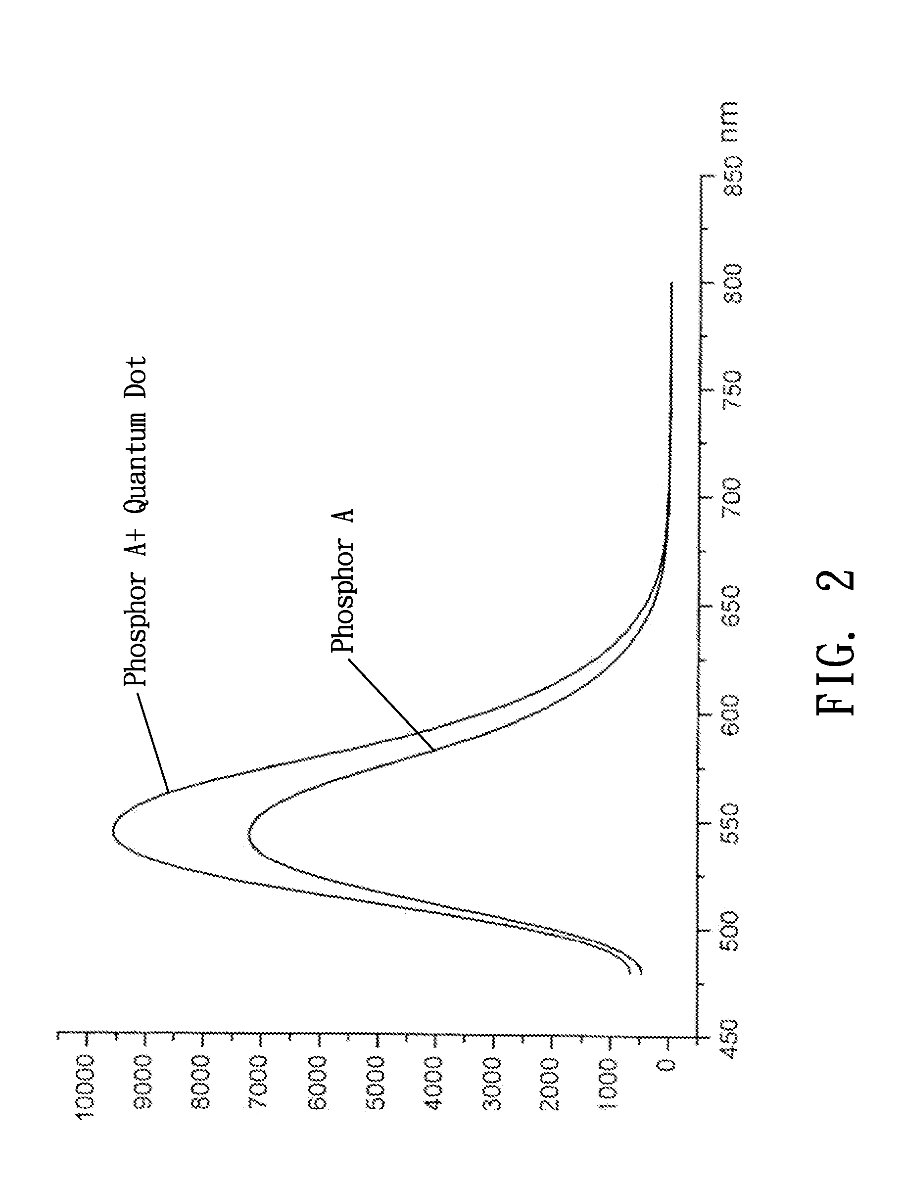
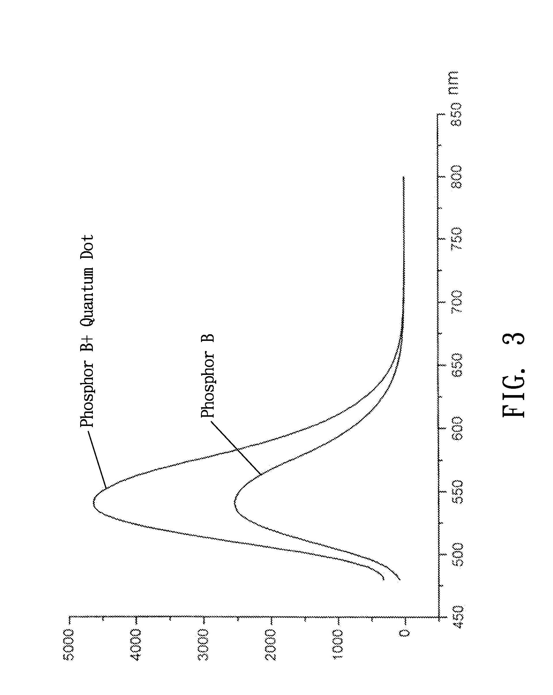
[0024]A compound material for inorganic phosphor and white LED in accordance with the present invention includes two inorganic substances, i.e., phosphor and light scatter, and a polymer adhesive. The compound material is used as a spectrum conversion film for interaction with a shortwave light radiated by an InGaN heterostructure, characterized in that the light scatter is a nano-scale powder material of AIIBVI quantum dot compound in which A=Zn, Cd; B═O, S, Se, Te, and composed with (Y2-x-y-zGdxCeyDyzO3)1.5±α(Al2O3)2.5±β inorganic phosphor to form a compound material. When compared to a standard phosphor binding object, the compound material re-radiates the light by a rise about 30˜70%, assuring emission spectrum maximum wavelength λ=542˜544 nm, radiation color coordinates 0.32□x□0.36, 0.32□y□0.38, and dominant wavelength λ□548 nm.

[0025]Further, the nano-scale powder material formed of AIIBVI quantum dot compound of the light scatter is based on (CdS)1˜p(CdSe)p series, raising Ful...


PUM

PropertyMeasurementUnit
quantum efficiencyaaaaaaaaaa
optical porosityaaaaaaaaaa
sizeaaaaaaaaaa

Abstract

A compound material for white LED, including an inorganic phosphor, an inorganic light scatter and a polymer adhesive for interaction with a shortwave light radiated by an InGaN heterostructure. The light scatter is a nano-scale powder material formed of AIIBVI quantum dot compound in which A=Zn, Cd; B═O, S, Se, Te, and composed with (Y2-x-y-z GdxCeyDyzO3)1.5±α(Al2O3)2.5±β inorganic phosphor to form a compound material.

Description

BACKGROUND OF THE INVENTION[0001]1. Field of the Invention[0002]The present invention relates to compound materials for LED and inorganic phosphor and more particularly, to a quantum effect-based radiator for used in an InGaN heterostructure semiconductor[0003]2. Description of the Related Art[0004]Some discoveries in physics in the technical field of “Optoelectronics” or “Solid State Light Sources” started in 70's of 20th Century. These discoveries were not employed for useful application at the time they were firstly disclosed or 15 years after their disclosure. A certain time thereafter, Japanese engineer S. Nakamura (please refer to S. Nakamura, G. Fasol “The blue laser diode” Sp˜Verl.B. 1997) discovered and described substantial improvement of InGaN shortwave heterojunction in internal and external quantum outputs.[0005]Thus, high performance blue, violet and ultraviolet LED samples were firstly reacted in 1997. On the same year, Nichia researchers disclosed white LED (see S. S...

Claims


Application Information

Patent Timeline
Patent Type & Authority Applications(United States)
IPC IPC(8): C09K11/02C09K11/70
CPCC09K11/7774H01L2933/0091H01L33/502H01L2224/48091H01L2224/48247H01L2224/48257H01L2924/00014
Inventor NAUM, SOSHCHINLO, WEI-HUNGTSAI, CHI-RUEI
Owner LO WEI HUNG
Learn More