Semiconductor device and method for manufacturing thereof

a semiconductor device and semiconductor technology, applied in semiconductor devices, semiconductor/solid-state device details, electrical devices, etc., can solve the problems difficult to increase the yield in the mounting process, and packages are prone to thermal deformation, so as to achieve the effect of increasing the mounting density of semiconductor devices

Active Publication Date: 2009-11-26
MONTEREY RES LLC
View PDF10 Cites 34 Cited by
  • Summary
  • Abstract
  • Description
  • Claims
  • Application Information

AI Technical Summary

Benefits of technology

[0011]A semiconductor device according to another aspect of the present invention includes: a stack of a plurality of semiconductor devices; and a conductive pin that penetrates through the recessed portion provided on the lead frame and the opening provided in the resin section of each of the plurality of semiconductor devices, so as to electrically couple the plurality of semiconductor devices with each other. According to this aspect of the present invention, a plurality of semiconductor devices can be mechanically and electrically coupled to each other by the conductive pin. Accordingly, a plurality of semiconductor devices can be stably stacked, whereby the mounting density of the semiconductor devices can be increased.
[0015]According to some aspects of the present invention, by inserting the conductive pin into the recessed section provided on the lead frame through the opening provided in the resin section, a plurality of semiconductor devices can be mechanically and electrically coupled to each other. Accordingly, a plurality of semiconductor devices can be stacked stably, whereby the mounting density of the semiconductor devices can be increased.

Problems solved by technology

However, increasing the mounting density of semiconductor devices remains an issue.
For example, a semiconductor device having a chip-on-chip structure has a problem that chips are prone to breakage and chips which are stacked are unable to be isolated for repair or disposal, subsequently making it difficult to increase the yield in the mounting process.
Conversely, a semiconductor device having a package-on-package structure has a higher yield compared to the semiconductor device having a chip-on-chip structure, however packages are prone to be thermally deformed due to soldering when stacking, and, unfortunately stably stacking a plurality of semiconductor devices according to conventional techniques can be extremely difficult.
Therefore, increasing the yield in the mounting process is difficult, and can result in increasing costs.
Furthermore, since the semiconductor chips need to be made smaller in order to increase the density, defectives are likely to be produced during manufacturing process.
In the semiconductor device having a package-on-package structure, yield is susceptible to decrease due to thermal deformation as the number of the stacked semiconductor packages increases.
Therefore, increasing the mounting density of the semiconductor devices is difficult.

Method used


Image

  • Semiconductor device and method for manufacturing thereof
  • Semiconductor device and method for manufacturing thereof
  • Semiconductor device and method for manufacturing thereof

Examples


first embodiment

[0047]With reference to FIG. 3 to FIG. 5, a method for manufacturing a semiconductor device 100 according to a first embodiment of the present invention will be described. With reference to FIG. 3A, an upper surface of a lead frame 10 comprised of, for example, copper or stainless steel is half-etched to form a recessed portion 12. The thickness of the lead frame 10 is preferable to be 100 μm to 200 μm. After half-etching, the thickness of the lead frame 10 at the recessed portion 12 is preferable to be 50 μm or less.

[0048]With reference to FIG. 3B, on a lower surface of the lead frame 10, a tape 50 with an adhesive for fixing the lead frame 10 is attached. A material of the tape 50 is preferable to be a polyimide-based resin with high thermal resistance, and the adhesive is preferable to be a silicon-based resin. With reference to FIG. 3C, a semiconductor chip 30 having an upper surface on which a circuit is formed is mounted, via an adhesive 34, on a base portion (metal plate 36) ...

second embodiment

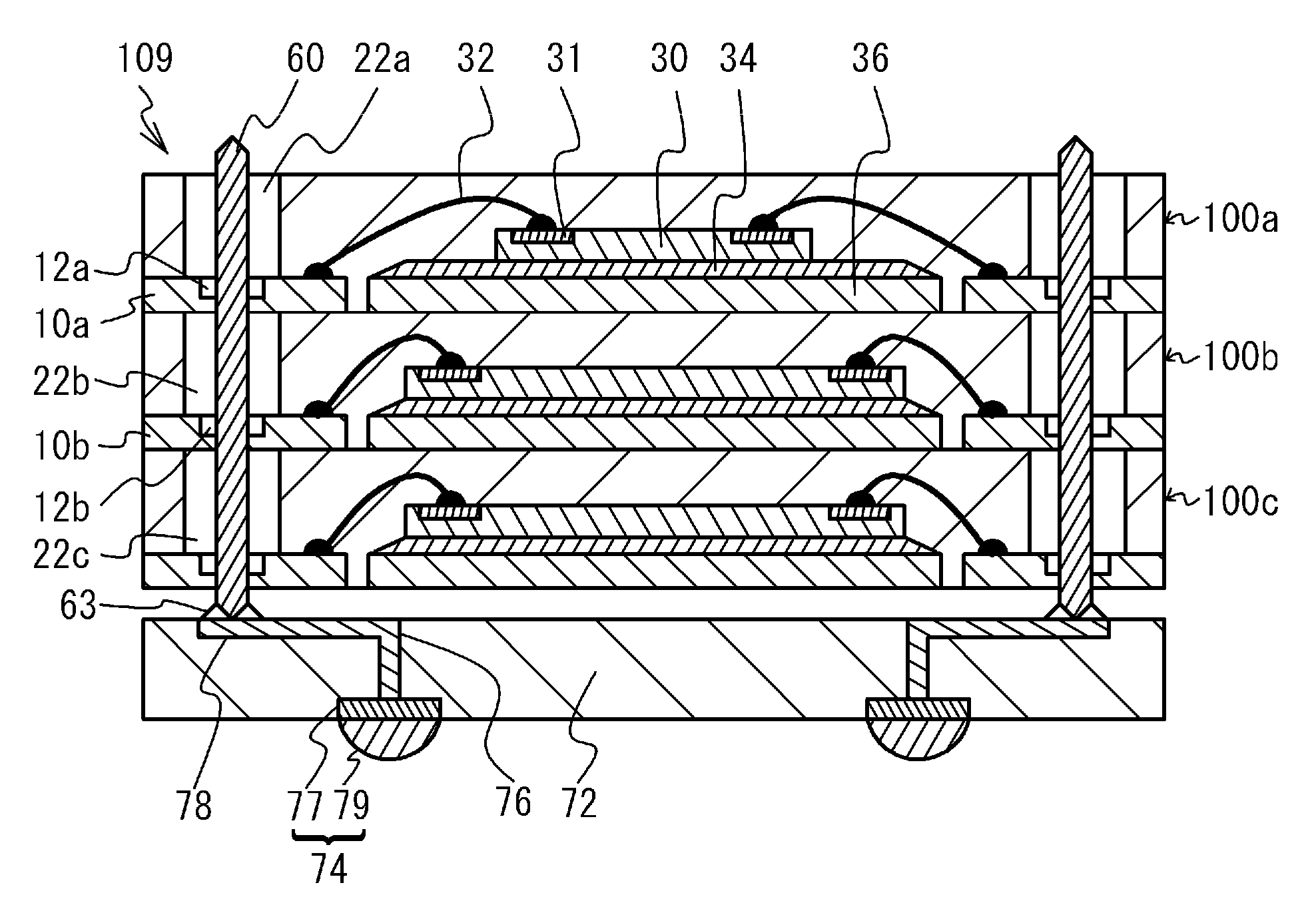
[0059]A second embodiment of the present invention is an exemplary semiconductor device provided with a recessed portion on a lower surface of a lead frame. FIG. 8A is a top view of a semiconductor device 102 according to the second embodiment, and FIG. 8B is a cross-sectional view taken along the line A-B-C-D-E-F of FIG. 8A. A recessed portion 14 is provided on the lower surface of the lead frame 10. The resin section 20 molds the lead frame 10 and the upper surface of the semiconductor chip 30. The opening 22 is provided above the recessed portion 14. A region 15 at the upper surface of the lead frame 10 that corresponds to (that is on the under side of) the recessed portion 14 is exposed to the outside through the opening 22. Other structures correspond to similarly numbered structures of the first embodiment (FIG. 6A and FIG. 6B).

[0060]With the semiconductor device 102 according to the second embodiment, by inserting the conductive pin 60 into the region 15 through the opening 2...

third embodiment

[0063]A third embodiment of the present invention is an exemplary semiconductor device provided with a through hole in a part of a recessed portion. FIG. 9A is a top view of a semiconductor device 103 according to the third embodiment. FIG. 9B is a cross-sectional view taken along the line A-B-C-D-E-F of FIG. 9A. The recessed portion 12 is provided with a hole 16 that penetrates through the lead frame 10. Other structures are the same as those of the first embodiment (FIG. 6).

[0064]According to the semiconductor device 103 of the third embodiment, the recessed portion 12 is provided with the hole 16 that penetrates through the lead frame 10. Accordingly, compared to the semiconductor device 100 discussed in the first described embodiment, the conductive pin 60 (see FIG. 7) can penetrate through the lead frame 10 with greater ease. Further, the hole 16 can be used as a marker for positioning when inserting the conductive pin 60, whereby the conductive pin 60 can be inserted with grea...


PUM


Abstract

The present invention provides a semiconductor device including: a semiconductor chip; a lead frame provided with a recessed portion on at least one of an upper surface or a lower surface thereof, and electrically coupled to the semiconductor chip; and a resin section that molds the semiconductor chip and the lead frame, and is provided with an opening above the recessed portion. By inserting a conductive pin (not shown) into the recessed portion through the opening, a plurality of semiconductor devices can be mechanically and electrically coupled to each other.

Description

CLAIM OF PRIORITY[0001]This application claims priority from Japanese patent application 2007-277998 filed on Oct. 25, 2007TECHNICAL FIELD[0002]The present invention particularly relates to a semiconductor device for stacking a plurality of semiconductor devices and a method for manufacturing the same.BACKGROUND ART[0003]Recently, to meet the demand for electronic equipment which are both compactly sized and highly functional, a number of technologies for increasing the mounting density of semiconductor devices have been developed. Such technologies include a semiconductor device having a chip-on-chip structure and a semiconductor device having a package-on-package structure.[0004]FIG. 20 of WO 99 / 56313 shows a semiconductor device in which a plurality of semiconductor packages are stacked by means of a solder ball provided on the tip of a through electrode provided on a lead frame. Published Japanese Translation of PCT Application No. JP-T-2000-510993 discloses a method for mountin...

Claims


Application Information

Patent Timeline
Patent Type & Authority Applications(United States)
IPC IPC(8): H01L23/495H01L21/56
CPCH01L23/49517H01L23/49548H01L24/97H01L25/105H01L2224/32145H01L2224/48227H01L2224/48465H01L2224/49171H01L2224/73265H01L2224/97H01L2924/01013H01L2924/01029H01L2924/01047H01L2924/01079H01L2924/01082H01L2924/15311H01L24/48H01L2924/01005H01L2924/01006H01L2924/01033H01L24/49H01L2924/3511H01L2224/32245H01L2224/48247H01L2225/1029H01L21/50H01L23/495H01L2224/85H01L2924/00H01L2924/00012H01L2924/181H01L24/73H01L2224/48464H01L2224/45015H01L2224/45147H01L2224/45144H01L2924/00014H01L24/45H01L2924/18165H01L2924/20751H01L2924/20752
Inventor MEGHRO, KOUICHIKASAI, JUNICHI
Owner MONTEREY RES LLC
Why Eureka
Try Eureka