Display device and method of producing the same

a technology of a display device and a production method, which is applied in the direction of instruments, other domestic objects, synthetic resin layered products, etc., can solve the problems of deteriorating production yield, difficult handling of glass substrates with less than 0.5 mm thickness, and constraints in view of film forming temperature, so as to prevent both strain and crack enlargement, improve image quality, and reduce production costs.

Active Publication Date: 2009-11-26
MITSUBISHI ELECTRIC CORP
View PDF3 Cites 45 Cited by
  • Summary
  • Abstract
  • Description
  • Claims
  • Application Information

AI Technical Summary

Benefits of technology

[0016]It is an object of the present invention to provide a display device and a method of producing the same in which image quality, reliability, durability, and yield are improved by preventing both strain and crack enlargement from being generated in a substrate.

Problems solved by technology

However, a glass substrate having a thickness less than 0.5 mm is difficult to handle at the time of production because it is bent under its own weight or a crack is easily generated.
Thus, a production yield deteriorates.
However, since the upper temperature limit of the resin film substrate is 200° C., there are constraints in view of a film forming temperature, etc.
According to the liquid crystal display device produced by using the thin glass substrate from the beginning of the production, or thinning the glass substrate during the production, the problem is that the thin glass substrate is distorted.
Since the gap between the substrates, that is, the thickness of the liquid crystal layer at the distorted part differs from that of the other part, or since the opposed substrates are displaced, the image quality deteriorates.
In addition, according to the production method for producing many devices at once, the problem is that a fine crack (microscopic crack) is generated at the cut part, that is, the cut end part of the substrate.
The microscopic crack could be a large crack when the substrate is curbed, for example.
In addition, it is reported that the crack becomes large rapidly when water enters into the microscopic crack.
Since the microscopic crack cannot be discovered by visual inspection or even by microscopic inspection in some cases, it could be a large crack while the liquid crystal display device is used.
In addition, not only the microscopic crack generated when the substrate is cut, but also a crack generated at the end part of the substrate caused by various reasons during the production process could be a larger crack.
Here, the above problems could arise in a display device other than the liquid crystal display device, and in a substrate formed of a material other than a glass material.

Method used


Image

  • Display device and method of producing the same
  • Display device and method of producing the same
  • Display device and method of producing the same

Examples


first embodiment

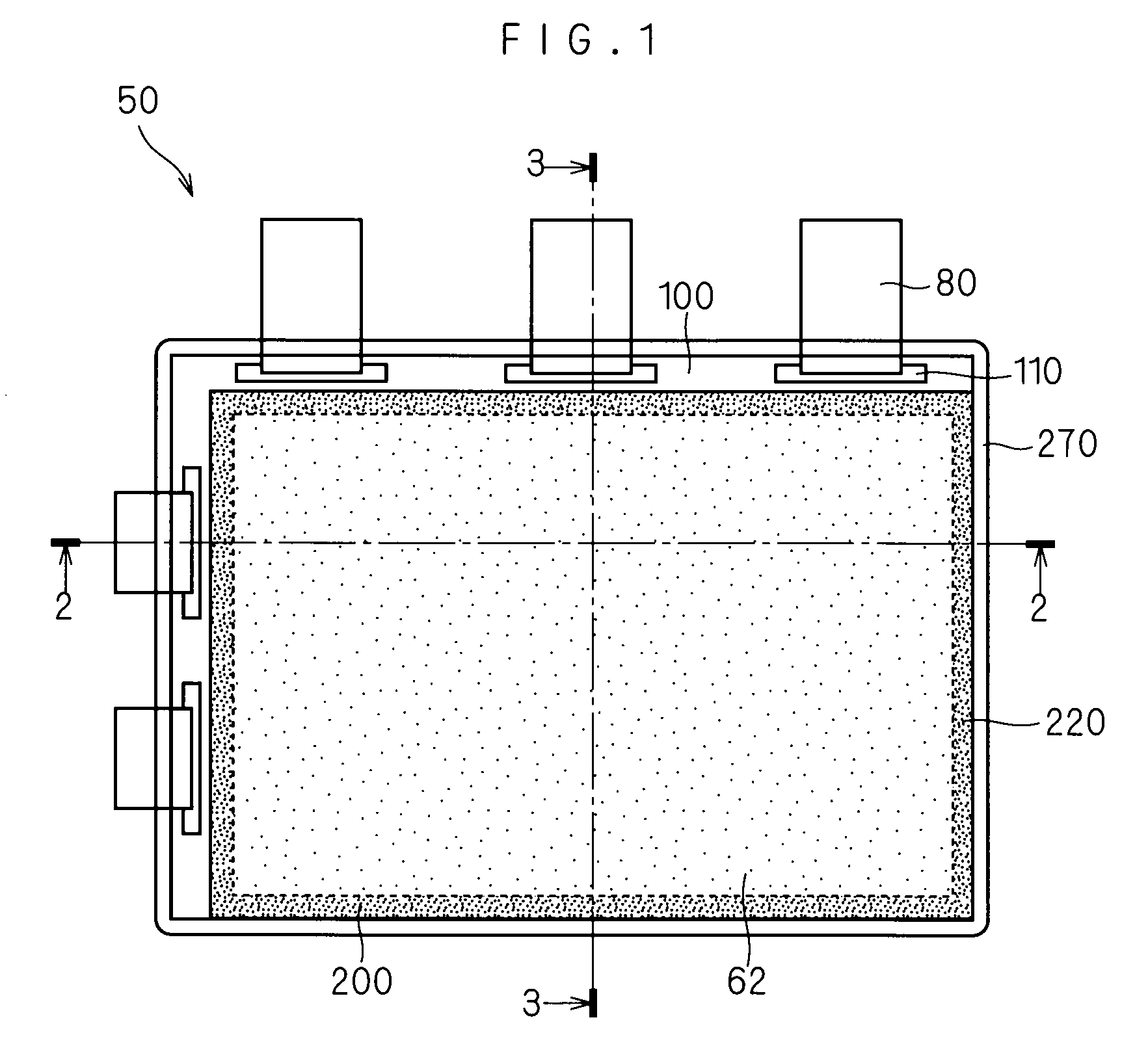
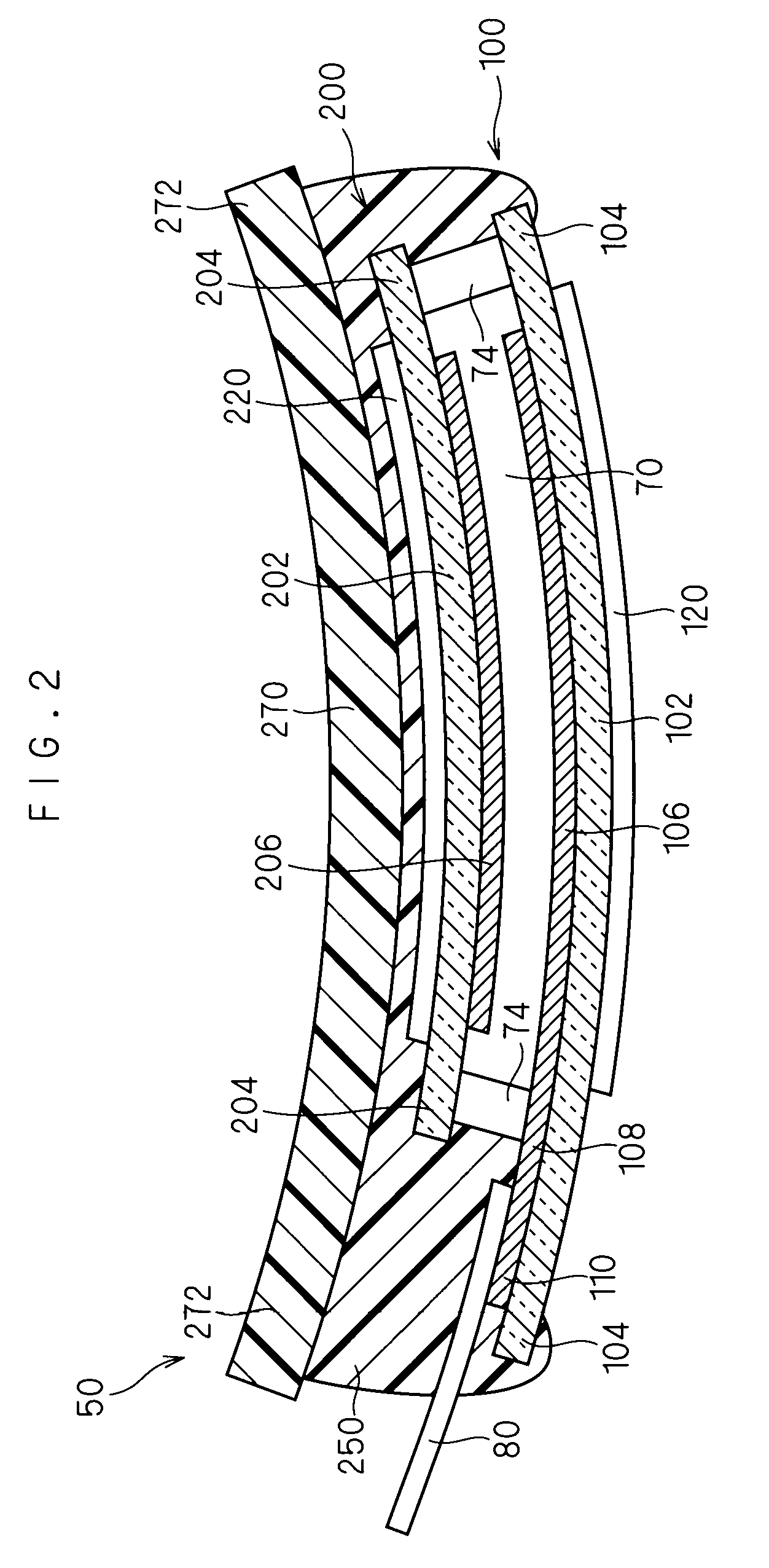
[0033]FIGS. 1 to 3 illustrates a liquid crystal display device 50 as one example of a display device according to a first embodiment of the present invention. FIG. 1 is a plan view, FIG. 2 is a sectional view taken along line 2-2 in FIG. 1, and FIG. 3 is a sectional view taken along line 3-3 in FIG. 1.

[0034]In addition, although one example of a TN (Twisted Nematic) type is used as the liquid crystal display device 50 here, the liquid crystal display device 50 may have another structure of the TN type or may have a structure (FFS (Fringe Field Switching) type or IPS (In-Plane Switching) type and the like) different from the TN type. In addition, although the case where the liquid crystal display device 50 is a color display type is illustrated, it can be a single color display type.

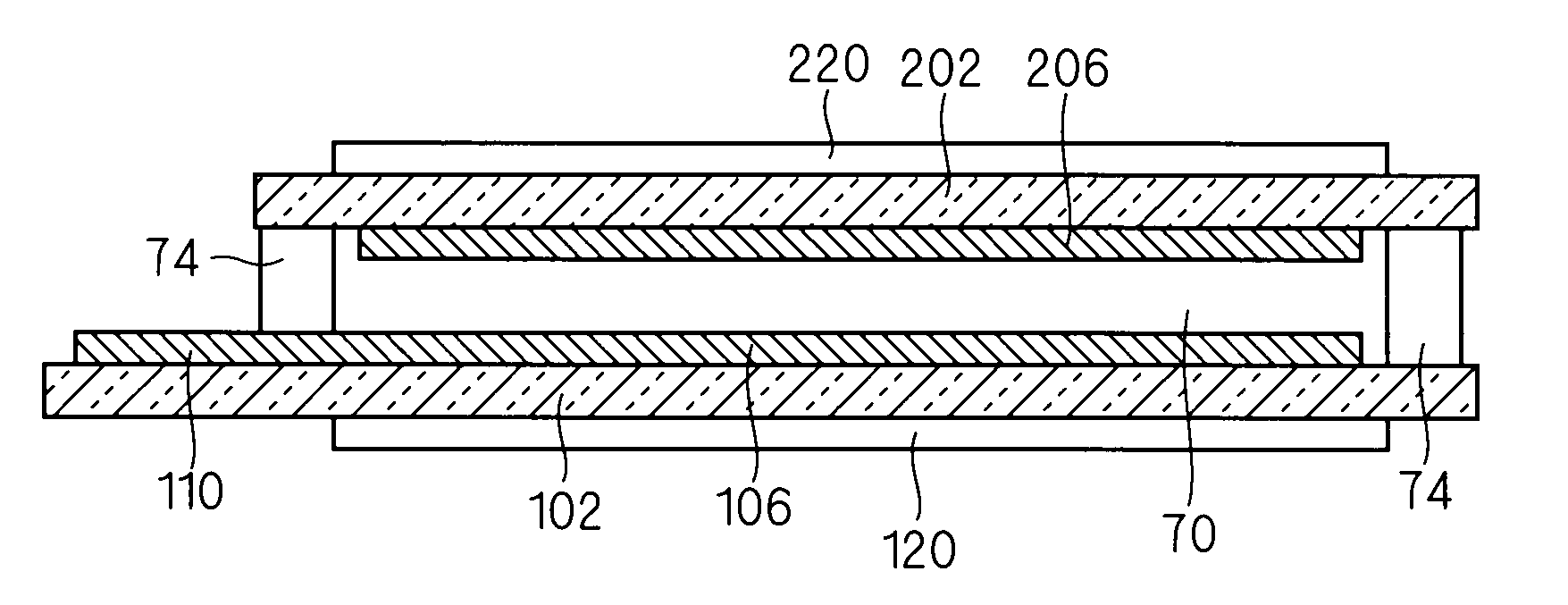
[0035]The liquid crystal display device 50 illustrated in FIGS. 1 to 3 includes a pair of insulating substrates 102 and 202, a liquid crystal (or liquid crystal layer) 70, and a seal 74.

[0036]Each of the ...

second embodiment

[0091]According to the structure of the liquid crystal display device 50 and production method thereof, the bonding agent 252 overflows to the projection part 272 of the strain suppressing plate 270 (see FIGS. 13 and 14). At this time, when the overflowing amount of the bonding agent 252 is small, the substrate end part 104 could not be covered with the bonding agent 252. Thus, according to a second embodiment, a production method adaptable to such a case and a liquid crystal display device 54 produced thereby will be described with reference to sectional views in FIGS. 20 to 23.

[0092]First, the structure shown in FIG. 12 is produced by the production method according to the first embodiment or another production method.

[0093]Then, as shown in FIG. 20, the liquid type or gel type bonding agent 252 is applied onto the polarizing plate 220, and the strain suppressing plate 270 is opposed to the insulating substrate 202 such that the strain suppressing plate 270 has the projection part...


PUM

PropertyMeasurementUnit
thicknessaaaaaaaaaa
temperatureaaaaaaaaaa
curvature radiusaaaaaaaaaa

Abstract

The display device includes a pair of insulating substrates arranged so as to be opposed, a bonding layer, and a strain suppressing plate. The bonding layer is provided on the outer surface side of one insulating substrate. The strain suppressing plate has rigidity higher than that of the insulating substrate to suppress the strain caused by curving the insulating substrate. The strain suppressing plate is fixed to the insulating substrate by the bonding layer.

Description

BACKGROUND OF THE INVENTION[0001]1. Field of the Invention[0002]The present invention relates to a display device and a method of producing the same and, more particularly, to a display device and a method of producing the same in which reliability, durability, yield and the like are improved by preventing a strain and a crack from being generated in a substrate.[0003]2. Description of the Background Art[0004]Flat display devices represented by a liquid crystal display device (LCD) are used in various kinds of field because of characteristics such as light in weight, thin, and low power consumption. Among them, the liquid crystal display device is widely used in information devices represented by a personal computer. In addition, recently, the liquid crystal display device is widely used as a TV component and a conventional Braun tube is being replaced with it.[0005]Moreover, a display device having a self-luminous light element in a display area, an electroluminescent (EL) display ...

Claims


Application Information

Patent Timeline
Patent Type & Authority Applications(United States)
IPC IPC(8): G02F1/1333B32B37/00
CPCB32B38/1866B32B2037/243G02F2201/503B32B2457/202G02F1/133305B32B2309/10
Inventor NAKAHATA, TAKUMIOKUMURA, TAKANORIYAMAGATA, YUSUKENAKAGAWA, NAOKIAGARI, MASAFUMISATAKE, TETSUYAKOKOGAWA, TORUARITA, KENJI
Owner MITSUBISHI ELECTRIC CORP
Why Eureka
Try Eureka