Printed wiring board

a printing board and wiring board technology, applied in the association of printed capacitors, electrical apparatus construction details, printed circuit non-printed electric components, etc., can solve the problem of easy malfunction, suppress the decrease in the decoupling effect, and reduce the loss of power supply from the chip capacitor to the processor cor

Active Publication Date: 2009-11-26
IBIDEN CO LTD
View PDF4 Cites 79 Cited by
  • Summary
  • Abstract
  • Description
  • Claims
  • Application Information

AI Technical Summary

Benefits of technology

[0019]The printed wiring board of the present invention may further include chip capacitors which are disposed at the side of a surface having the mounting portion thereon and which are independently connected to each of the layered capacitors. In this structure, when the capacitance is not sufficient only in the layered capacitor, the chip capacitors can compensate for the shortage. As the length of the wiring between a chip capacitor and a processor core increases the decoupling effect decreases. In this case, however, since the chip capacitors are disposed at the side Of the surface having the mounting portion thereon, the length of the wiring between each of the chip capacitors and the corresponding processor core can be small, and thus a decrease in the decoupling effect can be suppressed. Furthermore, since each of the chip capacitors is connected to the corresponding processor core via the layered capacitor, a loss of the power supply from the chip capacitor to the processor core can be decreased.
[0020]The printed wiring board of the present invention may further include a stress relief portion which is provided below the mounting portion and which is made of an elastic material. In this structure, even when a stress due to a difference in thermal expansion or the like is generated between the multicore processor mounted on the mounting portion and the printed wiring board except for the stress relief portion, the stress relief portion absorbs the stress, and thus problems such as a decrease in the connection reliability and a decrease in the insulation reliability do not easily occur. When a ceramic is used as the high-dielectric layer of a layered capacitor, cracks are easily generated in the high-dielectric layer because of its small thickness and brittleness. However, the presence of the stress relief portion can prevent the generation of cracks.
[0021]In this case, the stress relief portion may be provided in only an area directly under the multicore processor mounted on the mounting portion. A problem of a stress due to a difference in thermal expansion or the like mainly occurs in the area directly under the multicore processor. Therefore, when the stress relief portion is provided on this area, the cost of the material can be reduced.
[0022]Examples of the material of the stress relief portion include, but are not particularly limited to, organic resin sheets such as a modified epoxy resin sheet, a polyphenylene ether resin sheet, a polyimide resin sheet, a cyanoester resin sheet, and an imide resin sheet. These organic resin sheets may contain a thermoplastic resin such as a polyolefin resin or a polyimide resin; a thermosetting resin such as a silicone resin; or a rubber resin such as styrene-butadiene rubber (SBR), acrylonitrile-butadiene rubber (NBR), or a urethane. These organic resin sheets may contain fibers, fillers, or flakes made of an inorganic material such as silica, alumina, or zirconia. The stress relief portion preferably has a Young's modulus in the range of 10 to 1,000 MPa. In the case where the Young's modulus of the stress relief portion is within the above range, even when a stress due to a difference in the coefficient of thermal expansion between the semiconductor device mounted on the mounting portion and the layered capacitors is generated, the stress can be relieved.

Problems solved by technology

Therefore, when the voltage of one of the processor cores varies, the variation affects the voltages of the other processor cores, and a problem of malfunctioning easily occurs.

Method used


Image

  • Printed wiring board
  • Printed wiring board
  • Printed wiring board

Examples


first embodiment

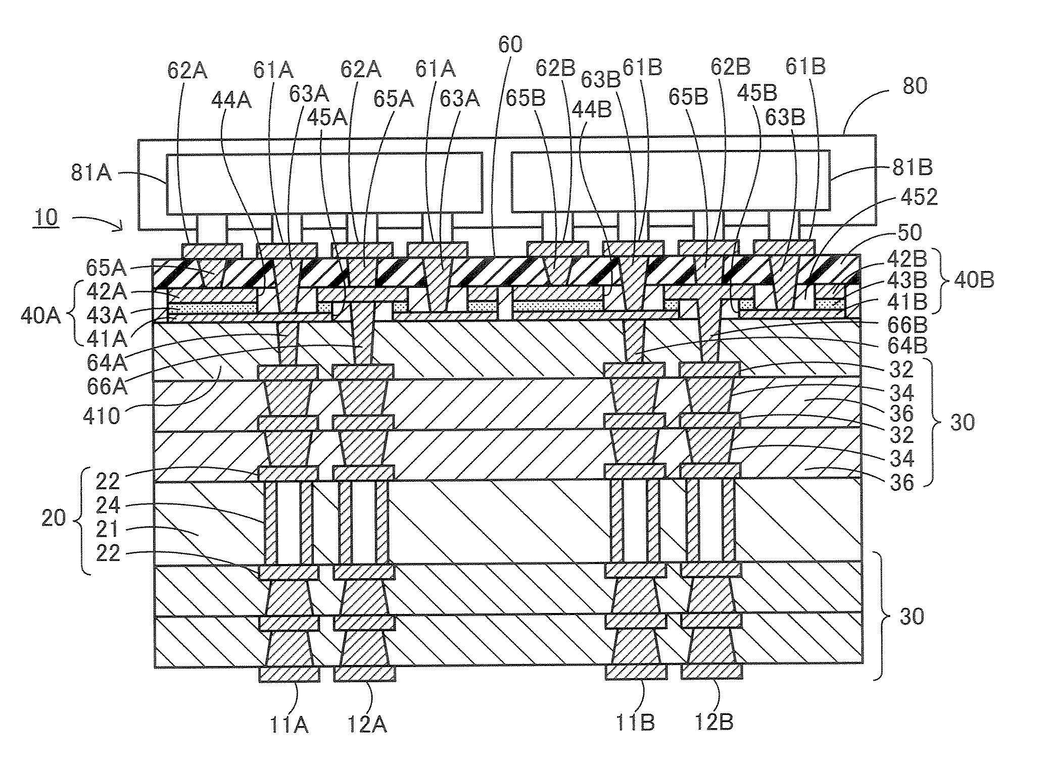
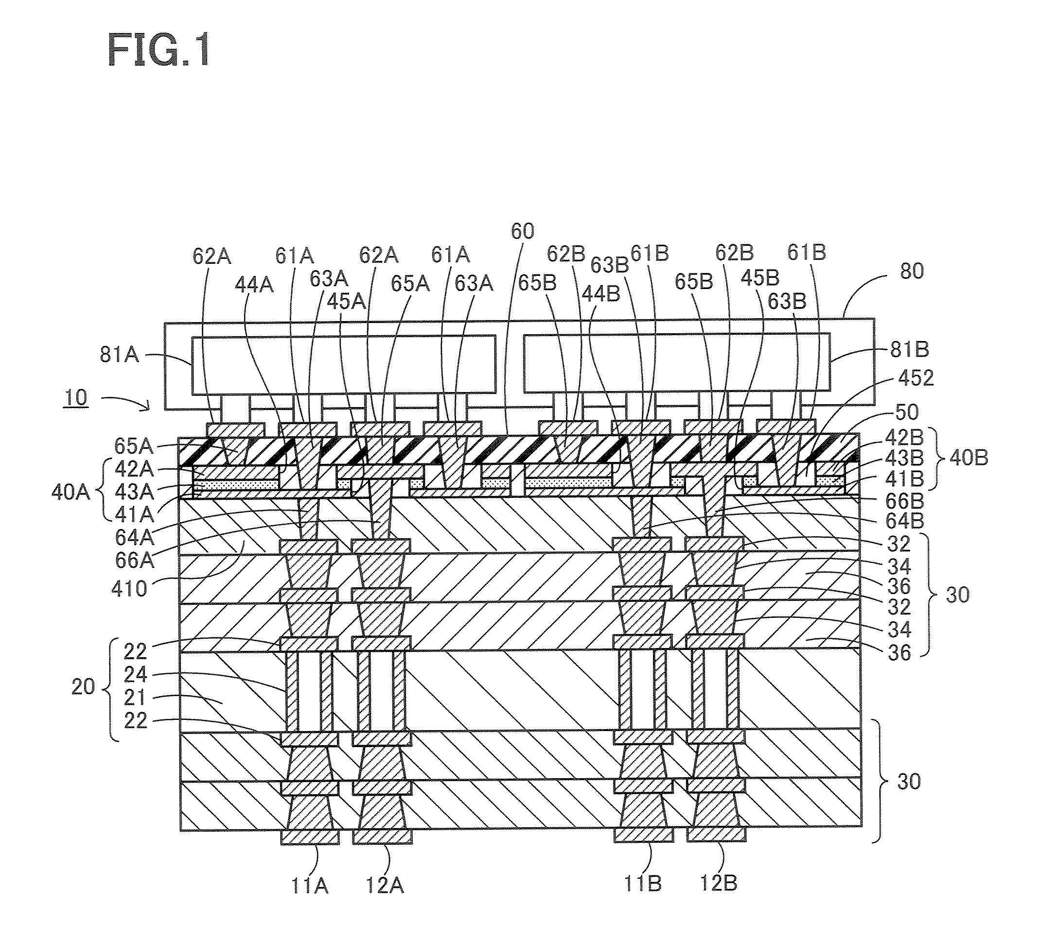
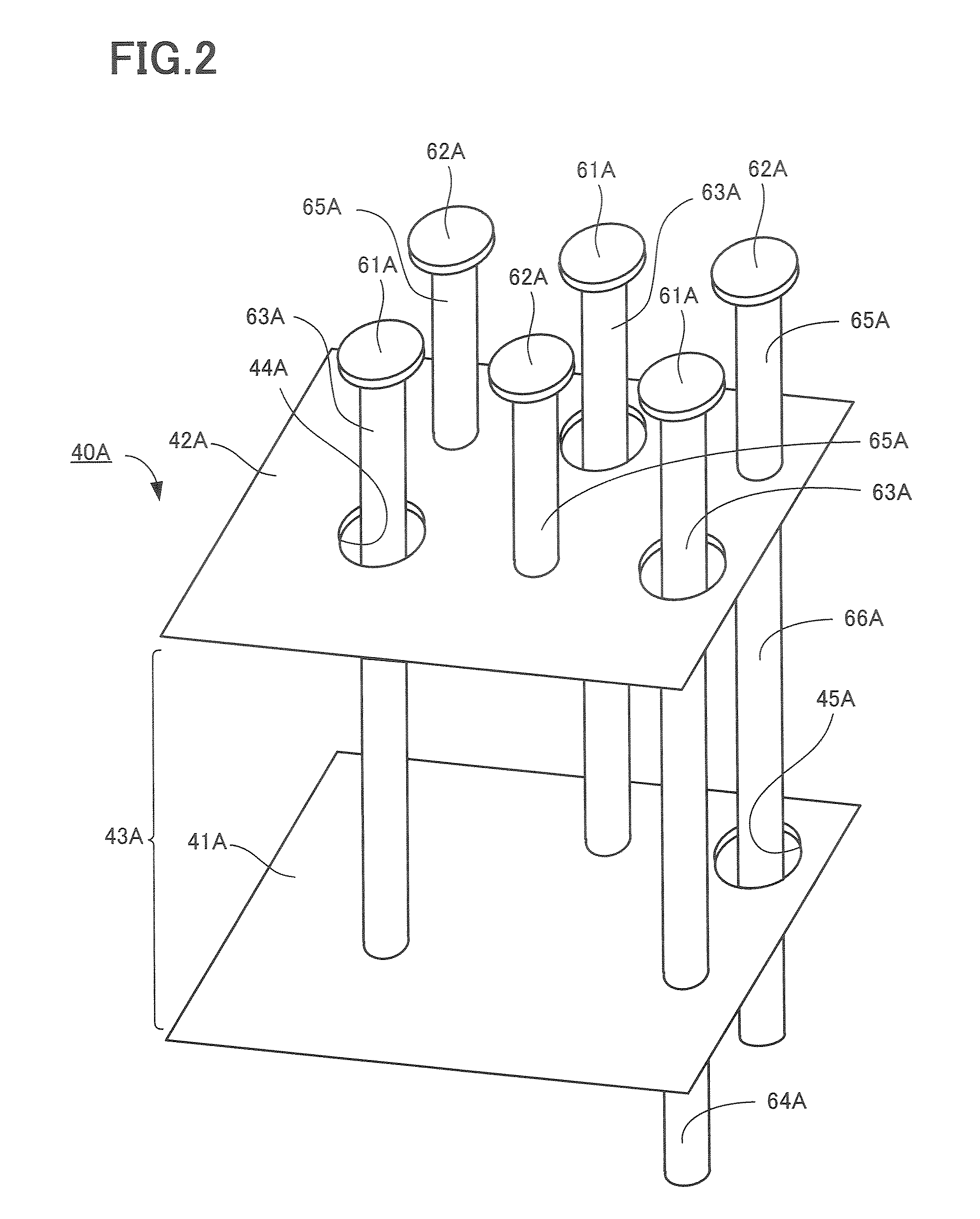
[0041]Embodiments of the present invention will now be described with reference to the drawings. FIG. 1 is a longitudinal cross-sectional view showing the overall structure of a multilayer printed wiring board 10 according to a first embodiment of the present invention. FIG. 2 is a schematic perspective view showing a first layered capacitor 40A.

[0042]The multilayer printed wiring board 10 includes a core substrate 20 in which wiring patterns 22 provided on the upper surface and the lower surface of the substrate are electrically connected to each other via through-hole conductors 24; built-up portions 30 in which a plurality of stacked wiring patterns 32 are electrically connected through resin insulating layers 36 through via holes 34, the built-up portions 30 being provided on each surface of the core substrate 20; a layered capacitor 40A which is provided on an interlayer insulating layer 410 provided on the upper surface of one of the built-up portions 30 and which includes a l...

second embodiment

[0070]FIG. 8 is a partial longitudinal cross-sectional view of a multilayer printed wiring board 110 according to a second embodiment. The multilayer printed wiring board 110 includes, as in the first embodiment, a mounting portion 160 on which a dual core processor 80 (see FIG. 1) including a first processor core 81A and a second processor core 81B in a single chip can be mounted, power supply lines that are independently provided for each of the processor cores, ground lines that are independently provided for each of the processor cores, and layered capacitors that are independently provided for each of the processor cores. Here, for convenience of description, a first layered capacitor 140A corresponding to the first processor core 81A will be mainly described. The structure of a second layered capacitor is substantially the same as that of the first layered capacitor 140A.

[0071]As shown in FIG. 8, the multilayer printed wiring board 110 of this embodiment includes an interlayer...

third embodiment

[0091]FIG. 13 is a partial longitudinal cross-sectional view of a multilayer printed wiring board 210 according to a third embodiment. The multilayer printed wiring board 210 includes, as in the first embodiment, a mounting portion 260 on which a dual core processor 80 (see FIG. 1) including a first processor core 81A and a second processor core 81B in single chip can be mounted, power supply lines that are independently provided for each of the processor cores, ground lines that are independently provided for each of the processor cores, and layered capacitors that are independently provided for each of the processor cores. Here, for convenience of description, a first layered capacitor 240A corresponding to the first processor core 81A will be mainly described. The structure of a second layered capacitor is substantially the same as that of the first layered capacitor 240A.

[0092]As shown in FIG. 13, the multilayer printed wiring board 210 of this embodiment includes an interlayer ...


PUM


Abstract

A printed wiring board includes a mounting portion on which a dual core processor including two processor cores in a single chip can be mounted, power supply lines, ground lines, and a first layered capacitor and a second layered capacitor that are independently provided for each of the processor cores, respectively. Accordingly, even when the electric potentials of the processor cores instantaneously drop, an instantaneous drop of the electric potential can be suppressed by action of the layered capacitors corresponding to the processor cores, respectively. In addition, even when the voltage of one of the processor cores varies, the variation in the voltage does not affect the other processor core, and thus malfunctioning does not occur.

Description

TECHNICAL FIELD [0001]The present invention relates to a multilayer printed wiring board including a built-up portion in which a plurality of wiring patterns that are stacked with insulating layers therebetween are electrically connected through via holes provided in the insulating layers.BACKGROUND ART [0002]Hitherto, various types of structures of a printed wiring board including a built-up portion in which a plurality of wiring patterns that are stacked with insulating layers therebetween are electrically connected through via holes provided in the insulating layers have been proposed. For example, in such a printed wiring board, when a semiconductor device mounted is switched between the on and off states at a high speed, switching noise may be generated, resulting in an instantaneous drop in the electric potential of a power supply line. In order to suppress such an instantaneous drop in the electric potential, connection of a capacitor portion between the power supply line and...

Claims


Application Information

Patent Timeline
Patent Type & Authority Applications(United States)
IPC IPC(8): H05K1/18
CPCH01L23/50H01L23/5383H01L2924/0001H01L2924/01012H01L2924/01084H01L23/5384H01L24/16H01L2224/16H01L2224/81192H01L2224/81815H01L2924/0102H01L2924/01025H01L2924/01046H01L2924/01057H01L2924/01078H01L2924/01079H01L2924/14H01L2924/15311H01L2924/19041H01L2924/19043H01L2924/30105H01L2924/30107H01L2924/3011H05K1/113H05K1/162H05K3/4602H05K3/4652H05K2201/0175H05K2201/0355H05K2201/09309H05K2201/09509H05K2201/09518H05K2201/096H05K2201/09718H05K2201/09763H05K2201/10674H01L2224/131H01L2924/01019H01L2924/014H01L2224/13099H01L2924/12042H01L2924/00014H01L2924/00011H01L2924/00H01L2224/0401H01L23/12H05K1/11
Inventor KARIYA, TAKASHI
Owner IBIDEN CO LTD
Why Eureka
Try Eureka