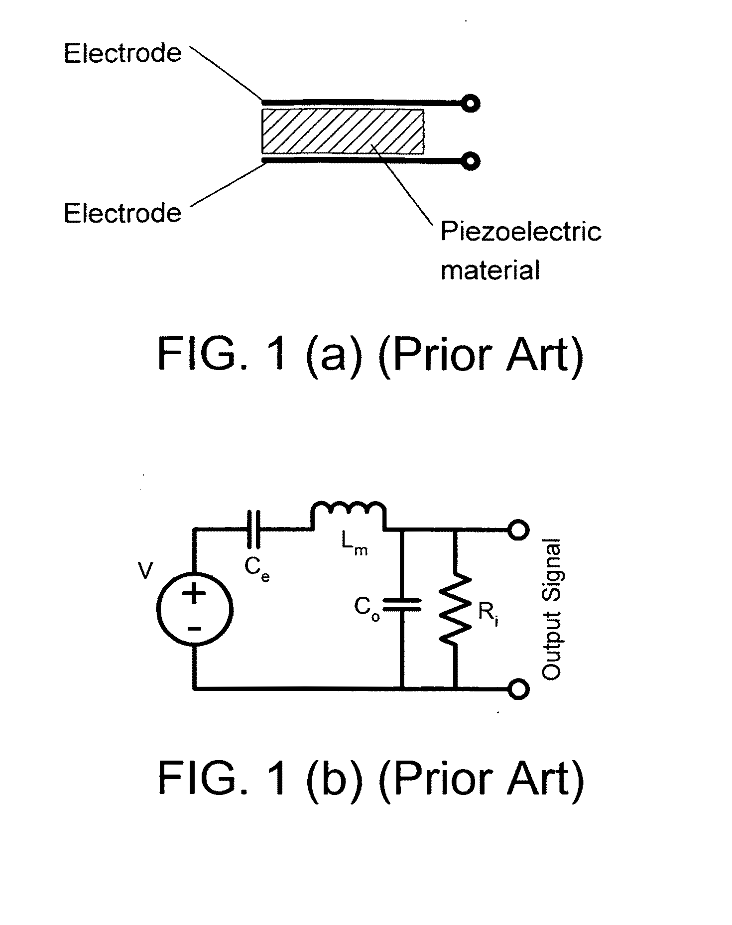
[0042]Piezoelectric effect is the ability of some materials (notably crystals and certain ceramics) to generate an electric potential in response to applied mechanical stresses. The effect finds useful applications such as the production and detection of sound, generation of high voltages, electronic frequency generation, microbalances, and ultra fine focusing of optical assemblies.
[0043]A piezoelectric sensor is a device that uses the piezoelectric effect to measure pressure, acceleration, strain or force by converting them to an electrical signal. FIG. 1(a) shows a simple piezoelectric sensor that is capable of generating an electrical charge in response to an external stress. Electrodes placed on the piezoelectric material detect the electrical charge when the piezoelectric material receives an external stress and the amount of the charge is related to the intensity of the stress. As shown in FIG. 1(b), a piezoelectric sensor can be modeled as a voltage source V that is directly proportional to the applied force, pressure, or strain. An output signal is then related to this mechanical force as if it had passed through an equivalent circuit. A model of this circuit includes the effects of the sensor's mechanical construction and other non-idealities. The inductance Lm is due to the seismic mass and inertia of the sensor itself. Ce is inversely proportional to the mechanical elasticity of the sensor. C0 represents the static capacitance of the sensor, resulting from an inertial mass of infinite size. Ri is the insulation leakage resistance of the sensor element.
[0044]Referring now to FIG. 2(a), when a thin layer of a piezoelectric material receives a stress ρ, for example when it is bent along the direction of the length (Direction 1), it generates an electrical charge Q in response to the stress. Depending on the property of the piezoelectric material, Q may be proportional to the amount of stress applied. Charge Q may be positive or negative. The polarity (+/−) of the charges generated can be used to indicate the direction of the bending (i.e. whether the bending curve is concave or convex).
[0045]Referring now to FIG. 2(b), if the stress ρ is in an arbitrary direction, it can be considered as having a component ρ1 in Direction 1 (in x axis), a component ρ2 in Direction 2 (in y axis) and a component ρ3 in Direction 3 (in z axis). A generated charge density D (=generated charge Q divided by active area A of the piezoelectric thin layer) by applied stress ρn (n=1, 2 or 3) can be described by Equation 1:
D = Q A = d 3 n ρ n ( n = 1 , 2 , or 3 ) ( 1 )
[0046]in which d is a piezoelectric coefficient.
[0047]The piezoelectric coefficient d may be different in different directions. This is called an anisotropic behavior. The anisotropic behavior of the piezoelectric materials mainly occurs in crystalline piezoelectric materials. In such materials, the generated charge varies depending on the direction that the stress is applied. The anisotropic behavior is described in the Equation 1 above by the direction-dependent piezoelectric coefficient d3n, in which n denotes the direction 1, 2 or 3.
[0048]Generally speaking, when a thin piezoelectric layer is bent, it forms a curvature κn. The applied stress ρn on the film is described by E-young's modulus of the film, l-thickness of the film, and κa-curvature of the layer, as depicted in Equation 2:
ρ n = El 2 κ n ( 2 )
[0049]Plugging Equation (2) into Equation (1), the curvature of the bending and the type of the bending (convex or concave) along the direction n can be determined by measuring the amount of the generated charge and charge polarity.
[0050]As can be seen from FIG. 2(b), when the piezoelectric thin layer is bent along an arbitrary direction, it forms a curvature κ1 in direction 1 (x axis) and a curvature κ2 in direction 2 (y axis). A cumulative charge Q is generated and it can be described by Equation 3:
Q = ElA 2 ( d 31 κ 1 + d 32 κ 2 ) ( 3 )
[0051]Therefore, a detected charge Q is the result of multidirectional stimulations and it presents a lump sum of the individual directional charges.
[0052]There is no limitation on bending directions. What is needed is a simplified model for solving such a lumped charge and to provide reasonable means to associate a particular charge to a particular direction of the stimuli. FIG. 2(c) shows an object with a surface S. Two sensing layers 1 and 2 are placed on the surface so that when the object is bent, the sensing layers 1 and 2 are also bent to the same extent. Assuming that due to the anisotropic behavior of the piezoelectric materials as mentioned above, sensing layer 1 is more sensitive (i.e. generates more electrical charge) when it is bent along the direction 1, while sensing layer 2 is more sensitive (i.e. generates more electrical charge) when it is bent along the direction 2. Directions 1 and 2 are not parallel to each other. If the object is bent along an arbitrary direction A as shown in FIG. 2(c), and if each sensing layer mostly responds to a stress in one direction, the layer 1 would generate a charge density D1 which is proportional to the stress component ρ1 in direction 1, and the layer 2 would generate a charge density D2 which is proportional to the stress component ρ2 in direction 2. The magnitude and polarity of the charge densities represent the degree and direction of the flexural deformation of the surface S at the location of the sensing layers.
[0053]Therefore, sensing a complex deformation of a surface can be achieved by placing one or more sensing devices on the surface. Each sensing device comprises two individual sensing layers stacked on top of each other. Each sensing layer is mostly sensitive to a single direction (sensing direction) and two of such directions are misaligned, preferably in a large angle or perpendicular to each other. By combining two (or more) predetermined sensing direction, it is possible to realize a system for detecting complex conformal deformations of the surface in 3D.
[0054]A sensor module is constructed based on the above principle. The sensor module comprises two sensing layers. Each sensing layer is a thin film made with a piezoelectric material. Each thin film layer comprises a large number of high aspect ratio piezoelectric crystallites called nanowires. The nanowires are aligned in a certain direction. This sensing layer can be made, for example, by applying a liquid dispersion of the nanowires on a substrate and, under an applied electrical field, dry the liquid content to bind the nanowires with a hosting material. The hosting material can be a polymer, or any similarly soft and flexible materials. Other techniques for aligning the nanowires can also be employed, as long as they are effective and practical.
[0055]The sensing materials suitable for the invention include zinc oxide (ZnO) nanowires, barium titanate (BaTiO3) nanowires, or carbon nanotube (CNT), etc. These nonowires or nanotubes should have a high length-to-diameter aspect ratio. For example, aspect ratio (length/diameter) of ordinary ZnO nanowires is anywhere from 10 to 1000 (typically ˜5 μm long by 50 nm diameter), which makes them inherently sensitive to the bending along the length. By an internal alignment of the nanowires in one predefined direction, the piezoelectric layer would be extremely sensitive to the bending along the direction of the alignment. In other words, axis of the alignment of the nanowires determines the axis of sensitivity against bending.
[0056]In very minimum, the sensor module of the present invention comprises one functional unit, namely one cell. A cross sectional view of the cell is shown in FIG. 3. This cell 100 comprises a top electrode 10, a first sensing layer 20, a central electrode 30, a second sensing layer 40, and a bottom electrode 50. The first sensing layer 20 and the second sensing layer 40 comprise aligned piezoelectric nanowires. The alignment direction of the nanowires in the first sensing layer 20 and the second sensing layer 40 should at least not be parallel to each other, preferably they are in a large angle or perpendicular to each other.
[0057]When an external stress is applied on the cell to cause a deformation (bending) of the cell, in response to the bending, the first sensing layer 20 generates a first voltage V1 between the top electrode 10 and the central electrode 30, or a resistance R1 between the top electrode 10 and the central electrode 30 changes an amount ΔR1. Likewise, the second sensing layer 40 generates a second voltage V2 between the bottom electrode 50 and the central electrode 30, or a resistance R2 between the bottom electrode 50 and the central electrode 30 changes an amount ΔR2. V1 (or ΔR1) and V2 (or ΔR2) are measurable by circuit 35 connected to the top electrode 10 and the central electrode 30, and by circuit 55 connected to the central electrode 30 and the bottom electrode 50, respectively. Depending on the bending direction, positive/negative (+/−) charges are generated. It is thus possible to determine the direction (convex/concave) of the bending and curvature of the bending.
[0058]The sensor module of the present invention may be constructed with multiple cells. For example, the cells in the sensor module may be arranged as a two-dimensional array (N columns×M rows; N, M≧1) as shown in FIGS. 4, 5 and 6. Referring now to FIG. 4, the sensor module 1000 comprises a top electrode layer 100, a first sensing layer 200, a central electrode layer 300, a second sensing layer 400, and a bottom electrode layer 500. The top electrode layer 100 comprises a first number (N) of strip electrodes arranged parallel to each other in a first direction (e.g. along the y direction). The bottom electrode layer 500 comprises same number (N) of parallel strip electrodes arranged in the same y direction as the top electrode layer 100. Each strip electrode in the top electrode layer 100 is aligned with a respective strip electrode in the bottom electrode layer 500 across the sensing layers so that a pair of top and bottom strip electrodes covers a column of cells (see illustration in FIG. 6). The central electrode layer 300 comprises a second number (M) of parallel strip electrodes arranged in a second direction (e.g. along the x direction). The number M may be same or different from number N. Each strip electrode in the central electrode layer 300 crosses every strip electrode in the top electrode layer 100 and the bottom electrode layer 500 so that it covers a row of cells (see illustration in FIG. 6). The strip electrode layers 100, 300 and 500 may be made, for example, by patterning high conductivity metal strips on a flexible thin film substrate.
[0059]Referring now to FIG. 5, although not required, sensing layers 200 and 400 can be continuous throughout the sensor module. The alignment directions of the nanowires in sensing layers 200 and 400 with respect to the directions of the strip electrode layers are not limited, as long as the nanowire alignment direction of the first sensing layer 200 and the second sensing layer 400 are not parallel to each other. A conventional arrangement is to have these two directions perpendicular to each other. For example, as shown in FIG. 5, the nanowires in the first sensing layer 200 may be arranged to be parallel to the strip electrodes of the first electrode layer 100 in the y direction. The nanowires in the second sensing layer 400 may be arranged to be parallel to the strip electrodes of the central electrode layer 300 in the x direction. Therefore, the sensor module of the present invention contains a set of two inherently aligned piezoelectric nanowire layers capable of detecting and allocating charges for particular axes and enable detection and monitoring of complex flexural deformation in 3D.
[0060]Further, soft and conductive materials may be used to fill the space between the nanowire layers and the strip electrode layers to provide mechanical integrity of the dispersed piezoelectric nanowires and enhance the charge collection efficiency from the nanowires towards the strip-electrodes.
[0061]Referring now to FIG. 6, the array of sensing cells is networked by a double x-bus readout architecture. The strip electrodes in the top electrode layer 100 are individually connected to a first x-bus 150. The strip electrodes in the bottom electrode layer 500 are individually connected to a second x-bus 550. The strip electrodes in the central electrode layer 300 are individually connected to a y-bus 350. Buses 150, 350 and 550 are connected to a control circuit 750. For a cell (i, j) of the sensor module 1000, the control circuit 750 is configured to measure a pair of voltages V1(i, j) and V2(i, j) in which:
V1(i,j)=Vti−Vcj
V2(i,j)=Vbi−Vcj
[0062]where Vti is the voltage of the ith strip electrode in the top electrode layer 100, Vbi is the voltage of the ith strip electrode in the bottom electrode layer 500, and Vcj is the voltage of the jth strip electrode in the central electrode layer 300.
[0063]When an external stress causing deformation is applied in vicinity of the cell (i, j), at least one of the voltages V1(i, j) and V2(i, j) is responsive to the intensity of the external stress. Data taken from the voltage measurement of the cells can be used in tracking flexural deformation of the sensor module. If the sensor module is placed in close contact with a surface, the flexural deformation of the surface may be measured by the sensor module.
[0064]Alternatively, instead of measuring voltages, resistance change in cells of the sensor module can also be used for tracking the flexural deformation. Referring again to FIG. 6, for a cell (i, j) of the sensor module 1000, the control circuit 750 may also be configured to measure a pair of resistances R1(i, j) and R2(i, j) in which R1(i, j) is the resistance between the ith strip electrode in the top electrode layer 100 and the jth strip electrode in the central electrode layer 300, R2(i, j) is the resistance between the ith strip electrode in the bottom electrode layer 500 and the jth strip electrode in the central electrode layer 300. When an external stress causing deformation is applied in vicinity of the cell (i, j), at least one of the changes of the resistances ΔR1(i, j) and ΔR2(i, j) is responsive to the intensity of the external stress. Data taken from the resistance change measurement of the cells can be used in tracking flexural deformation of the sensor module.
[0065]Further, the control circuit 750 may further be configured in such a way that the data measurement or readout is conducted repeatedly in a certain frequency so that the voltage or resistance data obtained are real-time data which can be used for measuring the deformation process in real time. For example, a sampling rate of ˜50 Hz may be used for real-time measurement with a reasonable accuracy.
[0066]Besides the two dimensional array type arrangement of the cells as described above, other shapes and arrangements of the sensor module are possible and they may be derived without departure from the scope of the invention. For example, the sensor module may be formed in a hollow tubular shape as shown in FIG. 7. The electrode layers, the sensing layers and possibly the readout buses may be arranged to be conform to the tubular shape. The tubular shaped sensor module is characterized by a radius r and a length L. Instead of using the x-y coordinates as mentioned above, a cell in the tubular sensor module may be described in two cylindrical coordinates z and φ, in which z is the distance from one end of the tube along the axis of the tube and φ is an angle.
[0067]Appropriate combination of the two voltage signals or two resistance change signals measured from a cell (z, φ) and application of certain mathematical transformation formulas provide for detection of the 3D complex conformal deformation of the tube (see Appendix 1 for information about the cylindrical coordinate system and transformation formulas).
[0068]Such a tubular shaped sensor module may be placed around a curved or cylindrical shaped surface for measuring the conformal deformation of the surface. FIG. 8(a) shows a contour map of skin deformation of a human hand. A hand gesture is represented by the skin deformation. The skin deformation may be detected and transformed into electrical signals for communication or device controlling. FIG. 8(b) shows a tubular shaped sensor module wrapping around a finger. The bending and movement of the finger may be detected by the sensor module and qualitatively transformed into electrical signals. The signals may be used as indicators for commanding an electronic device.
[0069]Because the sensor module can form many shapes possible, it can be particularly designed to fit a user's finger, arm, body, etc. The above-mentioned tubular shape is just one example. Other possible shapes and arrangements include gloves, wearable body wraps, flexible touch screens, balls, handles, etc. When a human body part that the sensor module is attached on moves, bends, squeezes or stretches, it causes the sensor module to produce certain electrical signals. If the sensor module is used as a user interface for an electronic device, the signals can be used for controlling the electronic device. Density of sensing elements (e.g. number of cells in a sensor module or number of cells in a unit area of a surface) determines the spatial resolution of the deformation measurement. In addition to using a single sensor module that comprises multiple cells, a plurality of sensor modules may be networked to form a system. A module or a system may comprise from a few cells towards hundreds of cells networked to form a so-called Flexural Sensing Layer (FSL). Right selection of cells and modules depends on the requirements for the final application and service. The simplest device might involve one or a few modules with moderate density of cells arranged on a strip, suitable for wrist watch-type user interface application, etc. Higher density of the cells (10/cm2) may be used for high resolution tracking of user skin deformation.
[0070]A computer program product may be used by the electronic device for controlling the interface of the present invention. The computer program product comprises at least a computer readable storage medium storing program codes thereon for use by the electronic device. The program codes comprise instructions for measuring V1(i, j) and V2(i, j) of the cell (i, j), or ΔR1(i, j) and ΔR2(i, j) of the cell (i, j), and instructions for calculating a flexural deformation as a result of an external stress. The measurement may be automatically repeated in a predetermined time interval. Data taken from the measurement of the cells can be used in tracking flexural deformation of the sensor module, or as command signals for controlling the electronic device.
[0071]It is to be understood that the above-described arrangements are only illustrative of the applications of the principles of the teachings hereof. In particular, it should be understood that although only a few examples have been shown, the teachings hereof are not restricted to those examples. Numerous modifications and alternative arrangements may be devised by those skilled in the art without departing from the scope of the present disclosure.
APPENDIX 1
Mathematical Transformation for Conformal Deformation Observation
[0072]As described, two sensing layers are placed between three layers of strip electrodes (top/central/bottom) to enable complex deformation detection of a surface by using two axes of single directional sensitivity (directions of sensitivity are marked as 1 and 2). Single directional sensitivity is enabled by highly aligned nanowires in the sensing layers. In other words, the axes of sensitivity determine two primary directions where conformal flexing can be depicted by κ1 and κ2 (curvatures of bending in direction 1 and 2, respectively). For the simplicity of mathematical operations, transformation into a cylindrical coordinate system is recommended. For instance, if the sensor module is wrapped around a cylinder (see FIG. 9), curvature of the sensing layers can be expressed as:
κ 1 = 1 + sin 2 θ 2 r κ 2 = 1 - sin 2 θ 2 r ( 4 )
where,
[0073]θ is angle of central axis of the sensing layer to central axis of cylinder,
[0074]r is radius of the cylinder,
[0075]κ1 and κ2 are curvatures along directions 1 and 2, respectively.
[0076]Sensing of complex deformation can be de-convoluted by using a system with two predetermined sensing directions (1, 2). These two directions are misaligned and can be perpendicularly placed to each other. In this case when external stress and deformation is applied on the sensing layer the radius and the angle of bending can be calculated as:
r = C 1 S 1 + S 2 and ( 5 ) θ = C 2 Sin - 1 ( C 3 S 1 - S 2 S 1 + S 2 ) ( 6 )
where (S1, S2) are directly measured variables (voltages and/or resistances) and C1, C2, C3 are calibration coefficients.