
Semiconductor Nanowire Vertical Device Architecture

Active Publication Date: 2009-12-03
QUNANO
View PDF4 Cites 27 Cited by
  • Summary
  • Abstract
  • Description
  • Claims
  • Application Information

AI Technical Summary

Benefits of technology

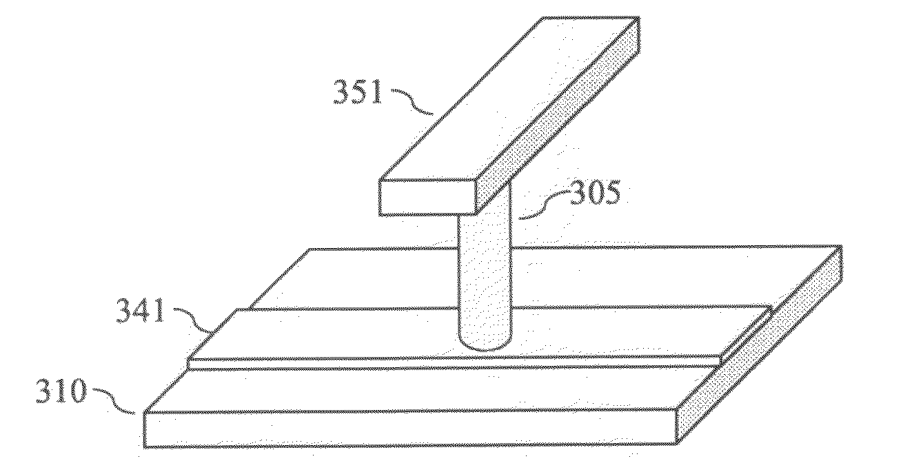
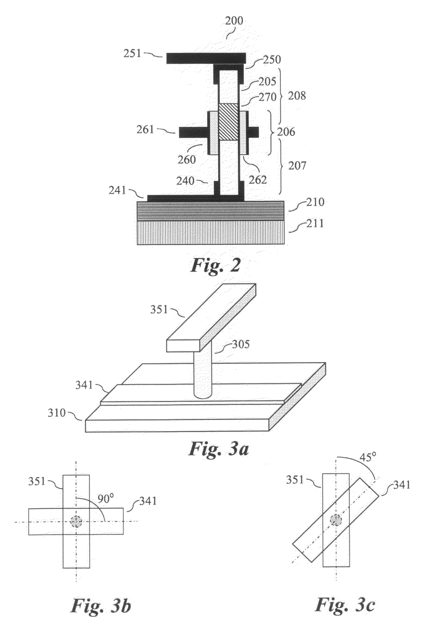
[0007]The nanoscaled electronic device according to the invention comprises one or a plurality of nanowires. The nanowires are the main functional part in the device, for example forming the current channel in a transistor. The nanowires have been formed vertically from a substrate, for example by epitaxial growth. Contacts are arranged on the nanowire at different parts of the nanowire. In connection to the nanowire contacts are external electrodes, that connect at different levels, as seen from the substrate, of the device. The external electrodes are elongated, and typically and preferably stripe-like. According to the invention a first external electrode, or contacts, associated with contact(s) at a first part of the nanowire, and a second external electrode, associated with contact(s) at a second part of the nanowire are arranged in a cross-bar configuration. The cross-bar configuration minimizes the overlay of the external electrodes, hence, parasitic capacitances and current leakage can be avoided, or at least reduced. The contacts at a first part of the nanowire may for example be source contacts at the “root” of the nanowire and the contacts at a second part of the nanowire drain contacts at the top of the nanowire.
[0008]More levels of external electrodes can be introduced, for a example a external electrode level associated with a gate contact, in between the source and drain levels. The external electrodes can be arranged in a cross-bar configuration minimizing the overlay between the external electrodes at all levels. Alternatively the cross-bar configuration is pair-wise, minimizing the overlay between external electrodes at adjacent layers.
[0009]The most favorable architecture according to the invention is a perpendicular cross-bar geometry, i.e. the drain and source external electrodes forming an angle of around 90° then seen in the direction of the vertical nanowire. Even if other design constrains make it impossible to have an 90° angle between the external electrodes, a cross-bar geometry with an angle around 45° would efficiently limit the overlap and positively enhance the performance.
[0010]Thanks to the invention it is possible to provide electronic devices built around one or more nanowires with better performance, due to the better handling of parasitic capacitances and leakage currents.
[0011]Important advantages of the present invention include increased performance of diodes (speed and sensitivity), improved performance of transistors (speed and power handling), increased sensitivity of photodetectors, and increased performance of optical sources and detectors.

Problems solved by technology

Obviously the prior art design of vertical nanowire device need improvements with regards to parasitic influences from the external electrodes, the parasitic capacitances and increased leakage currents, arising therefrom, severely impairing the performance of the device.

Method used


Image

  • Semiconductor Nanowire Vertical Device Architecture
  • Semiconductor Nanowire Vertical Device Architecture
  • Semiconductor Nanowire Vertical Device Architecture

Examples


Embodiment Construction

[0022]The arrangement and architecture according to the present invention will be described with a wrap-gated nanowire field effect transistor as a non-limiting example. The wrap-gated nanowire transistor exemplifies a device which is sensitive to parasitic capacitances and / or current leakage. Other devices that would be effected in similar ways, include, but is not limited to: LEDs, other types of diodes, for example quantum mechanical resonant tunneling diodes, bipolar transistors, solar cells and sensors.

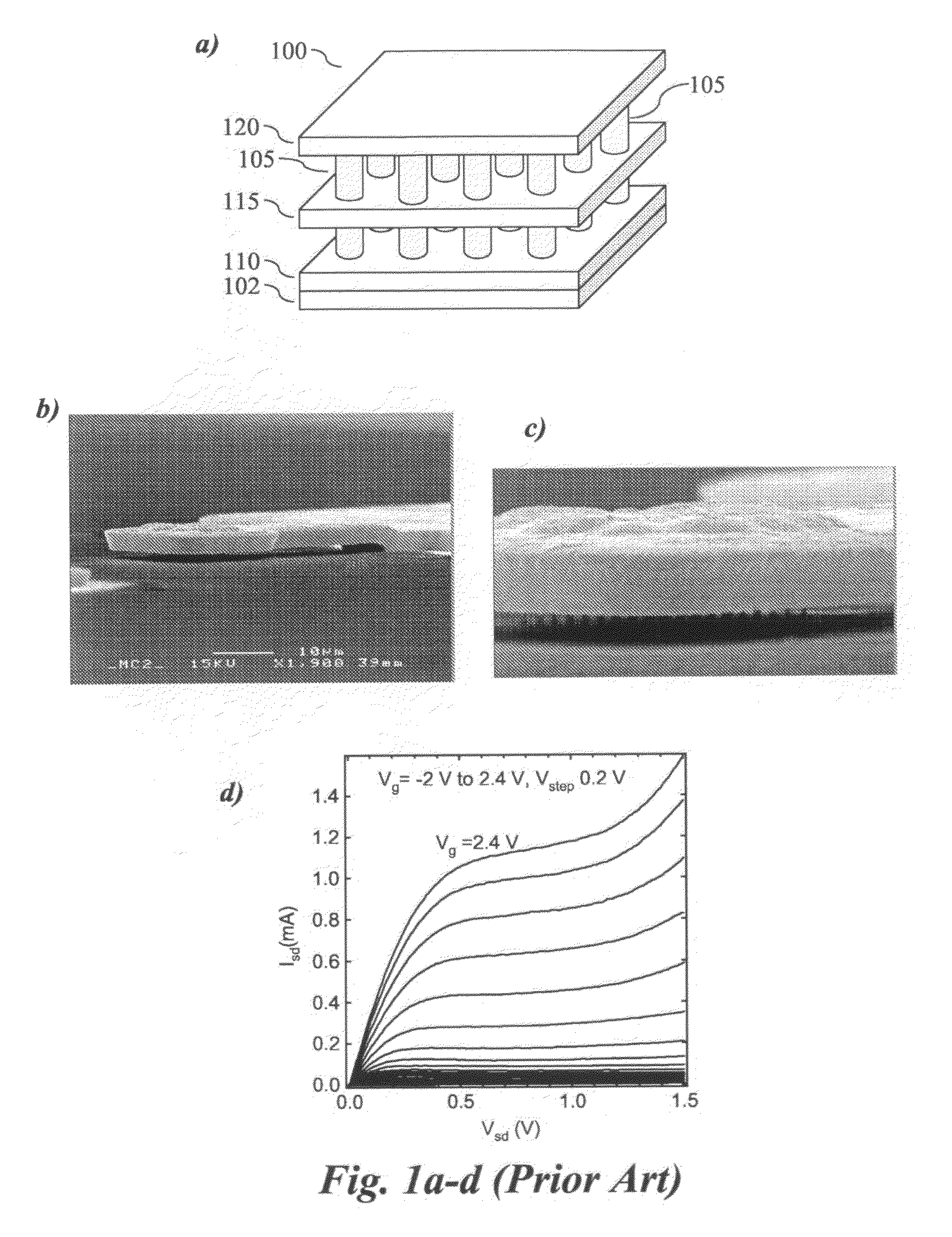
[0023]The functionality of a device according to FIG 1a is illustrated by the IV-characteristics of FIG. 1d. The device is a fabricated transistor using an airbridge technology for the drain formation, as illustrated in FIG. 1b-c. In this exemplary transistor ˜100 nanowires are placed in parallel between two plate electrodes. The device is fabricated by electron beam lithography (EBL). It has been shown that nanowires can also be grown from metal particles defined by nano imprint...


PUM


Abstract

The present invention relates to nanoscaled electronic devices with a vertical nanowire as a functional part. Contacts are arranged on the nanowire at different parts of the nanowire, for example drain and source contacts. In connection to the nanowire contacts are external electrodes, that connect at different levels, as seen from the substrate, of the device. The external electrodes are elongated, and typically and preferably stripe-like. According to the invention a first external electrode, or contacts, associated with contact(s) at a first part of the nanowire, and a second external electrode, associated with contact(s) at a second part of the nanowire are arranged in a cross-bar configuration. The cross-bar configuration minimizes the overlay of the external electrodes, hence, parasitic capacitances and current leakage can be reduced, and the performance of the device improved.

Description

TECHNICAL FIELD[0001]The present invention relates to a nanowire electronic device architecture. In particular the invention relates to arrangement of external electrodes connecting to terminals, or contacts, of the nanowire electronic device.BACKGROUND[0002]The interest in nanoscaled electronic devices has during the last decade increased substantially. The interest arises from the continuous need for denser integrated circuits, but also from the realization that nanoscale electronic devices offers new possibilities in terms of operational speed, functionality and power consumption, for example. These new possibilities, but also in some aspects new challenges, are primarily related to the exploration of quantum mechanical effects coming into importance as the size of devices go down to the nano-region. The scaling also allows for an materials integration that may not be achieved in the conventional technologies. Of particular interest are devices based on semiconductor nanowires. S...

Claims


Application Information

Patent Timeline
IPC IPC(8): H01L29/06H01L23/482B82B1/00
CPCB82Y10/00H01L29/0665H01L29/0673H01L29/775H01L29/068H01L29/165H01L29/205H01L29/0676
Inventor WERNERSSON, LARS-ERIKBRYLLERT, TOMASLIND, ERIKSAMUELSON, LARS
Owner QUNANO
Learn More