Nanobioelectronics

a technology of nano-electronics and micro-electronics, applied in the field of nano-electronics, can solve the problems of difficult multiplexing and lack of resolution necessary to provide fine-grain information at the level of individual cells

Inactive Publication Date: 2009-12-03
PRESIDENT & FELLOWS OF HARVARD COLLEGE
View PDF23 Cites 28 Cited by
  • Summary
  • Abstract
  • Description
  • Claims
  • Application Information

AI Technical Summary

Benefits of technology

[0010]In another aspect, the present invention is directed to a method of making one or more of the embodiments described herein, for example, an article comprising a nanoscale wire, and a cell in electrical communication with the nanoscale wire. In another aspect, the present invention is directed to a method of using one or more of the embodiments described herein, for example, an article comprising a nanoscale wire, and a cell in electrical communication with the nanoscale wire.
[0011]Other advantages and novel features of the present invent

Problems solved by technology

Micropipette electrodes can stimulate and record intracellular and extracellular potentials in vitro and in vivo with relatively good spatial resolution, yet are difficult to multiplex.
Microfabricated structures, such as electr

Method used


Image

  • Nanobioelectronics
  • Nanobioelectronics
  • Nanobioelectronics

Examples


example 1

[0082]The interface between nanoscale semiconductors and biological systems represents a powerful means for molecular-scale communication between these two distinct yet complementary components of information processing systems. This example illustrates the assembly and electrical properties of nanowire-based device arrays integrated with mammalian neurons. Discrete hybrid structures enable neuronal recording and stimulation at the axon, dendrite, or soma with high sensitivity and spatial resolution. Aligned arrays of these electronic nanostructures are used to measure the speed and shape evolution of action potentials as well as to interact with a single cell as multiple inputs and outputs. Additionally, we have demonstrated the assembly of hybrid n- and p-type structures enabling the generation of bipolar signals that could form the basis of logic gates and other integrated neuron-based computing structures. The flexible assembly of arrays of these structures creating tens of inpu...

example 2

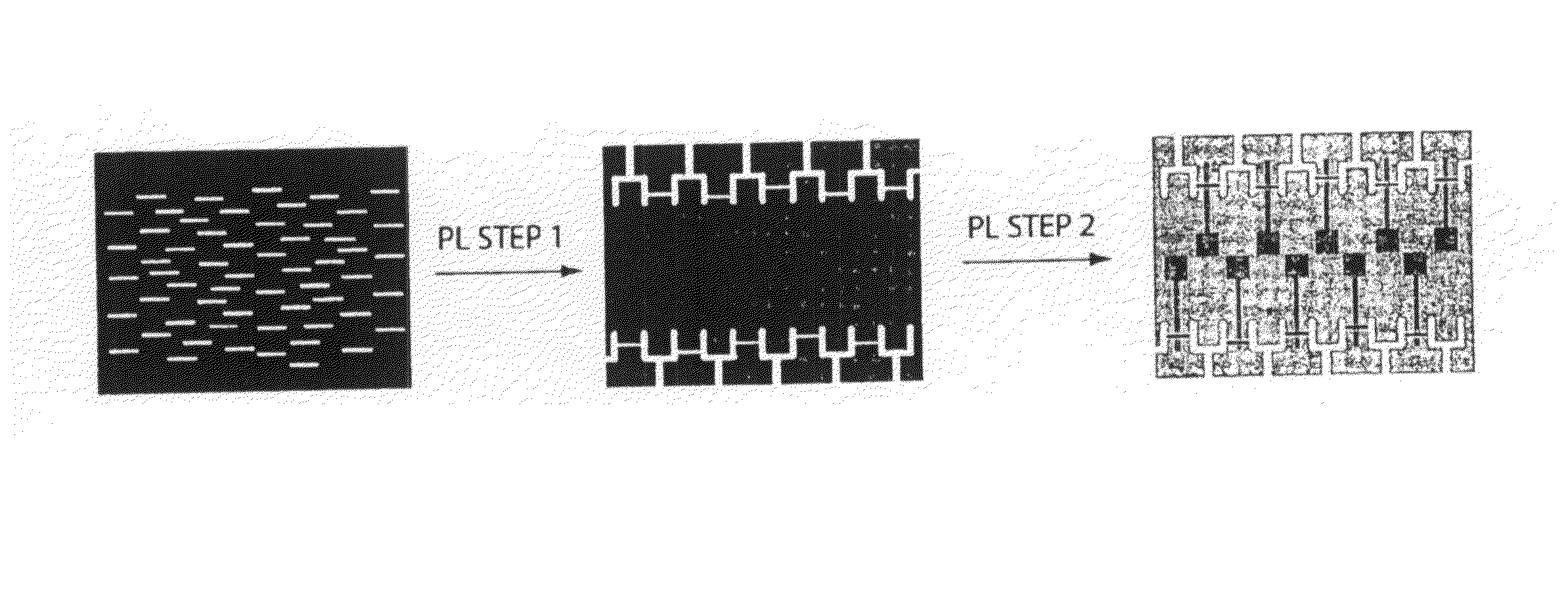
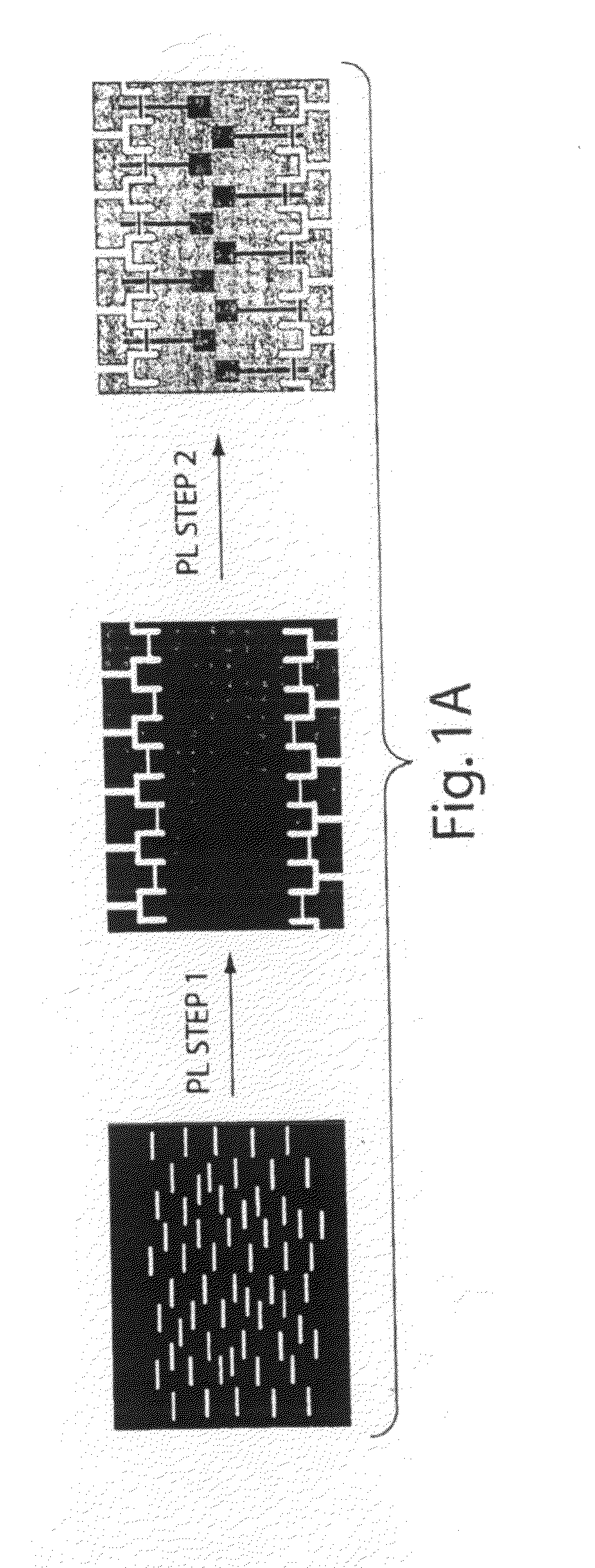
[0083]This example illustrates the preparation of certain nanowire / neuron devices, according to one embodiment of the invention. FIG. 1A is a general schematic for the preparation and assembly of oriented p- and / or n-type silicon nanowires in an aligned neuron / nanodevice array, with interconnection into well-defined FET device array structures, patterning of polylysine as an adhesion and growth factor to define neuron cell growth with respect to the device elements, and neuron growth under standard conditions (discussed in detail below). This approach is flexible allowing for variations in the addressable nanowire device separations down to at least 100 nm and device array geometry, incorporation of electronically distinct p- and n-type elements in well-defined positions, and / or variation in the number and spatial location of the hybrid nanowire / neuron junctions or synapses with respect to the cell body and neurite projections. Moreover, new chips incorporating such changes can be r...

example 3

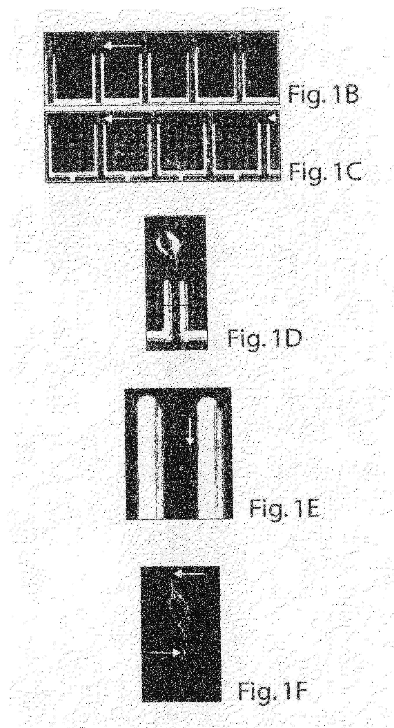
[0091]In this example, nanowire / soma and nanowire / dendrite hybrid structures were also investigated and found to exhibit excellent electrical communication. Intracellular stimulation of action potential spikes in the soma yielded correlated conductance peaks measured by the nanowire in a nanowire / soma structure (FIGS. 7A-7D). These figures show the silicon nanowire device before (FIG. 7A) and after (FIG. 7B) deposition and growth of a cortical neuron with the cell body over the nanowire device; the arrows highlight the positions of the nanowire and cell body, respectively. Also shown are intracellular (FIG. 7C) and nanowire (FIG. 7D) electrical responses of the neuron after intracellular current injection (arrows; 15 msec, 0.6 nA pulse).

[0092]The shape and width of the conductance peak (FIGS. 7E-7F) were similar to those determined from nanowire / axon structures. FIG. 7E is a graph showing representative electrical signals detected by nanowire devices for individual soma-nanowire con...


PUM


Abstract

The present invention generally relates to nanobioelectronics and, in some cases, to circuits comprising nanoelectronic elements, such as nanotubes and/or nanowires, and biological components, such as neurons. In one aspect, cells, such as neurons, are positioned in electrical communication with one or more nanoscale wires. The nanoscale wires may be used to stimulate the cells, and/or determine an electrical condition of the cells. More than one nanoscale wire may be positioned in electrical communication with the cell, for example, in distinct regions of the cell. However, the nanoscale wires may be positioned such that they are relatively close together, for example, spaced apart by no more than about 200 nm. The nanoscale wires may be disposed on a substrate, for example, between electrodes, and the cells may be adhered to the substrate, for example, using cell adhesion factors such as polylysine. Also provided in other aspects of the invention are methods for making and using such devices, kits for using the same, and the like.

Description

RELATED APPLICATIONS[0001]This application claims the benefit of U.S. Provisional Patent Application Ser. No. 60 / 783,203, filed Mar. 15, 2006, entitled “Nanobioelectronics,” by Patolsky, et al.GOVERNMENT FUNDING[0002]Research leading to various aspects of the present invention were sponsored, at least in part, by DARPA. The U.S. Government may have certain rights in the invention.FIELD OF INVENTION[0003]The present invention generally relates to nanobioelectronics and, in some cases, to circuits comprising nanoelectronic elements, such as nanotubes and / or nanowires, and biological components, such as neurons.BACKGROUND[0004]Electrophysiological measurements made using micropipette electrodes and microfabricated electrode arrays play an important role in understanding signal propagation through individual neurons and neuronal networks. Micropipette electrodes can stimulate and record intracellular and extracellular potentials in vitro and in vivo with relatively good spatial resoluti...

Claims


Application Information

Patent Timeline
IPC IPC(8): A61B5/05H01L29/66
CPCB82Y10/00G01N33/5058H01L29/1606H01L29/0673H01L29/0665
Inventor PATOLSKY, FERNANDOTIMKO, BRIAN P.YU, GUIHUALIEBER, CHARLES M.
Owner PRESIDENT & FELLOWS OF HARVARD COLLEGE
Why Eureka
Try Eureka