
Method, device, and program for simulating NANO substance in electric field

a nano substance and electric field technology, applied in nanoinformatics, instruments, computations using non-denominational number representations, etc., can solve the problems of inability to accurately predict the advantageous effect of electric field application, inability to describe electronic transportation by way of classical boltzmann transport equation, and inability to improve accuracy. , to achieve the effect of improving accuracy

Inactive Publication Date: 2009-12-03
NEC CORP
View PDF0 Cites 2 Cited by
  • Summary
  • Abstract
  • Description
  • Claims
  • Application Information

AI Technical Summary

Benefits of technology

[0005]Promotion of such researches strongly requires accurate prediction of the electronic property and the electric conduction in a case where a nano structure is actually in an electric field, and some advantageous effects are expected such as reduction in cost and time for trial and errors during repeated creation of a nano structure and a device-operation property.
[0006]Conventional simulation technologies for device operation were performed based on the classical Boltzmann transport equation by way of: extracting a necessary parameter from a band structure when executing a macro simulation with the simulation including dielectric constant, effective mass and relaxation time; and calculating, based on the classical electrodynamics, the field distribution relative to the assumed device structure.
[0007]In the case of Si material, improved accuracy was successfully achieved of the aforementioned effective mass approximation and relaxation time.
[0008]Non-patent Document 1: E. Runge and E. K. U. Gross, Phys. Rev. Lett. 52, 997 (1984)
[0009]Non-patent Document 2: J. Ihm, A. Zunger, and M. L. Cohen, J. Phys. C: Solid State Physics, Vol. 12, 4409 (1979) Non-patent Document: O. Sugino and Y. Miyamoto, Phys. Rev. B59, 2579 (1999); Phys. Rev. B66, 89901(E) (2002)DISCLOSURE OF THE INVENTIONProblem To Be Solved By the Invention

Problems solved by technology

However, the aforementioned prior arts contained the following problems.
The first problem is that since the channel length is in the nanoscale order, electronic transportation could not described by way of the classical Boltzmann transport equation.
This is because when the channel length is of nanoscale, the electronic transportation is shifted to ballistic transportation, and because accuracy could not improve unless the electronic transportation chases the real time evolution of the wave function of electrons when passing through portion of channel from the electrode.
The second problem is that the aforementioned prior arts make it difficult to accurately predict the advantageous effect of the electric field application.

Method used


Image

  • Method, device, and program for simulating NANO substance in electric field
  • Method, device, and program for simulating NANO substance in electric field
  • Method, device, and program for simulating NANO substance in electric field

Examples


embodiments

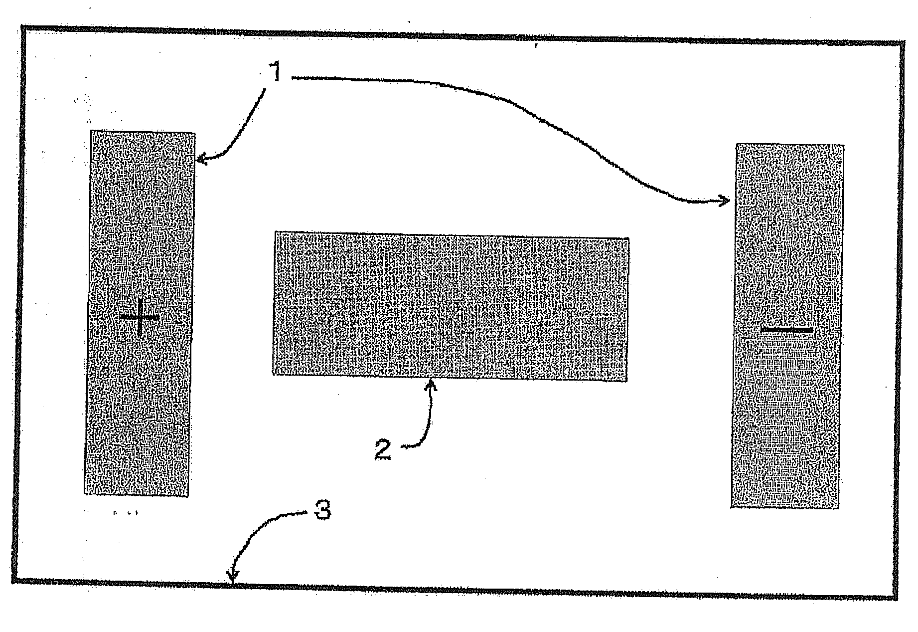
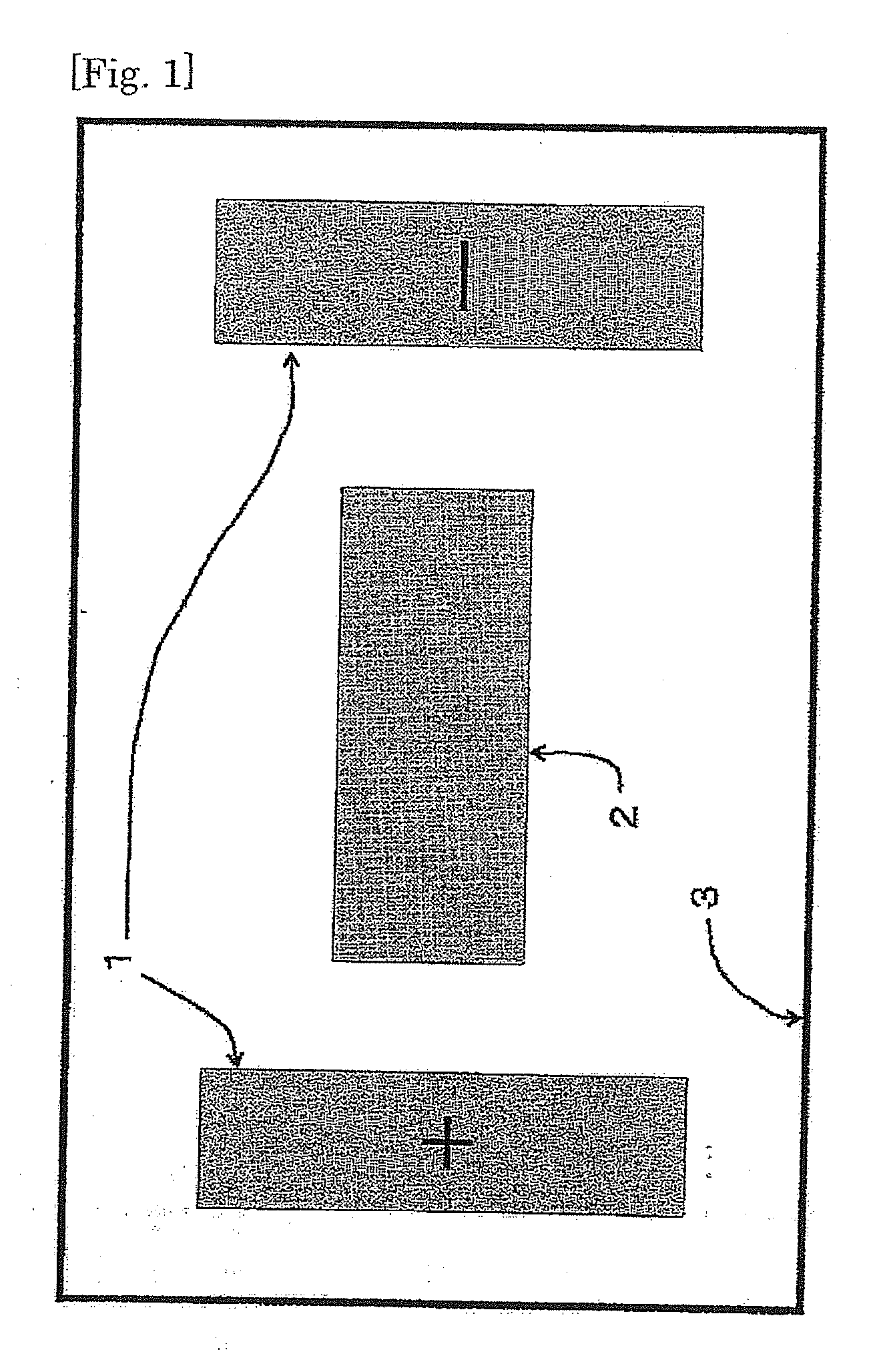
[0053]Referring to FIG. 1, the present Embodiment comprises a virtual charge distribution 1 that simulates the applied electric field, and a substance (material model) 2 that is calculated in ab initio calculation. The substance 2 contains a plurality of atoms (electrons, atomic nuclei) etc. the electronic state of which is to be analyzed (not shown).

[0054]The virtual charge distribution 1 can be optionally generated on a real-space mesh, and the charge distribution can be calculated by solving a Poisson equation. The simulation system according to the present Embodiment simulates a device either under a vacuum region condition or under a periodic boundary condition in which is assumed existence of a continuum dielectric, so that a potential distribution is calculated by way of Fourier-transforming a charge distribution into a reciprocal lattice space. The electric field strength distribution is equivalent to space derivative of the potential distribution. Meanwhile, in the present ...


PUM


Abstract

The present invention provides with a method for enabling a highly accurate simulation by calculating dynamical response of electrons in the electric field without using a “fitting parameter”. According to the present invention, the method for simulating a field distribution of a nano substance in an electric field comprises the step of a Fourier transform process by virtually applying a model on which a three-dimensional periodic boundary condition is imposed to the a field distribution of a nano substance in an electric field.Further, the method for simulating a field distribution of a nano substance in an electric field comprises the steps of arranging a virtual charge distribution on a space mesh, and evaluating a field distribution of a nano substance by calculating a potential distribution by way of Fourier-transforming a charge distribution into a reciprocal lattice space.

Description

TECHNICAL FIELD OF THE INVENTION[0001]The present invention relates to a simulator technique using a computer and, more particularly, to a method, a device and a program for simulating nano substance in an electric field.DESCRIPTION OF THE RELATED ART[0002]Aiming to more sufficiently describe the current technical level relating to the present invention, all of the patents, patent applications, patent publications, scientific articles and so on, which are cited or specified herein, are hereby incorporated by reference in their entirety.[0003]As indicated in the International Technology Roadmap for Semiconductors, a next-generation semiconductor having a semiconductor gate length of 30 nm of shorter is expected to be put to practical use after 2010.[0004]Further, researches have been actively conducted for practical application of new-generation electronic devices based on new nano substance as typified by a carbon nanotube.[0005]Promotion of such researches strongly requires accurat...

Claims


Application Information

Patent Timeline
IPC IPC(8): G06F17/11G06F17/14
CPCB82Y10/00H01L29/78H01L29/0673H01L29/0665
Inventor MIYAMOTO, YOSHIYUKI
Owner NEC CORP
Learn More