Method for producing silicon wafer

a manufacturing method and silicon wafer technology, applied in the direction of polycrystalline material growth, crystal growth process, protective fluid, etc., can solve the problem of deterioration of the physical properties of the device, the existence of such grow-in defects becoming intolerable, and the defect referred to as the “grown-in defect”

Active Publication Date: 2009-12-10
SUMCO TECHXIV
View PDF8 Cites 21 Cited by
  • Summary
  • Abstract
  • Description
  • Claims
  • Application Information

AI Technical Summary

Benefits of technology

[0029]It is therefore an object of the present invention to prevent slip from occurring starting from interstitial-type point defects, in a region of a silicon single crystal from its shoulder portion to the top part of its straight cylinder portion, when the silicon single crystal is pulled under growth conditions corresponding to the I-rich region.
[0030]It should be noted that none of the...

Problems solved by technology

However, a crystal defect referred to as the “grown-in defect” (defect incurred during the crystal growth) occurs in the course of the growth of a silicon single crystal.
Along with recent progress of integration and refinement of semiconductor circuits, the presence of such grow-in defects has become intolerable in the vicinity of a surface layer of a silicon wafer where ...

Method used


Image

  • Method for producing silicon wafer
  • Method for producing silicon wafer
  • Method for producing silicon wafer

Examples


Embodiment Construction

[0051]Embodiments of the present invention will be described with reference to the drawings.

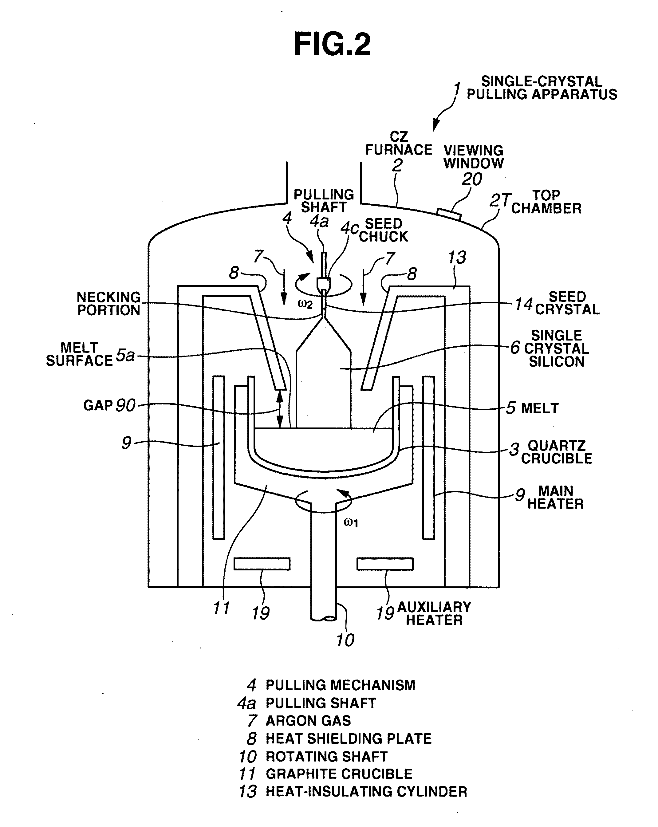
[0052]FIG. 2 is a diagram showing configuration of a silicon single crystal manufacturing apparatus for use in an embodiment, as viewed from a side.

[0053]As shown in FIG. 2, the single crystal pulling apparatus 1 according to the embodiment has a CZ furnace (chamber) 2 functioning as a single crystal pulling vessel.

[0054]A quartz crucible 3 is provided inside the CZ furnace 2 to contain molten polycrystalline silicon material as melt 5. The quartz crucible 3 is covered with a graphite crucible 11 arranged outside thereof. A main heater 9 is provided laterally outside of the quartz crucible 3 to heat and melt the polycrystalline silicon material within the quartz crucible 3. An auxiliary heater (bottom heater) 19 is provided in the bottom of quartz crucible 3 to supplementarily heat the bottom of the quartz crucible to prevent the hardening of the melt 5 in the bottom of the quartz crucible 3....


PUM


Abstract

A method for producing a silicon wafer in which occurrence of slip starting from interstitial-type point defects is prevented in a part from the shoulder to the top of the straight cylinder portion of a silicon single crystal when the silicon single crystal is grown by pulling method under growth conditions entering an I-rich region. In order to prevent occurrence of slip in the range from the shoulder (10A) to the top of the straight cylinder portion (10B), the silicon single crystal (10) is pulled under conditions that the oxygen concentration Oi from the shoulder (10A) to the top of the straight cylinder portion (10B) of the silicon single crystal (10) is not lower than a predetermined concentration for preventing slip starting from interstitial-type point defects, more specifically not lower than 9.0×10¹⁷ atoms/cm3.

Description

TECHNICAL FIELD[0001]The present invention relates to a method for manufacturing a silicon wafer without occurrence of slip.BACKGROUND ART[0002]A silicon single crystal is manufactured by pulling using the CZ (Czochralski) method. The pulled silicon single crystal ingot is sliced into silicon wafers. A semiconductor device is fabricated through a device process to form a device layer on the surface of a silicon wafer.[0003]However, a crystal defect referred to as the “grown-in defect” (defect incurred during the crystal growth) occurs in the course of the growth of a silicon single crystal.[0004]Along with recent progress of integration and refinement of semiconductor circuits, the presence of such grow-in defects has become intolerable in the vicinity of a surface layer of a silicon wafer where a device is fabricated. Thus, studies are being conducted on the possibility of producing a defect-free crystal.[0005]In general, there are the following three types of crystal defects which...

Claims


Application Information

Patent Timeline
IPC IPC(8): C30B15/20
CPCC30B29/06C30B15/206
Inventor KUROKI, HIDETOSHIYOSHINAGA, MOTOAKISHIRAISHI, YUTAKASHIBATA, MASAHIRO
Owner SUMCO TECHXIV
Why Eureka
Try Eureka