

Methods for Wafer Scale Processing of Needle Array Devices
a technology of array devices and wafers, applied in the field of wafer scale processing of needle array devices, can solve the problems of increasing manufacturing costs, slowing down production, and vast potential for implanting electronic devices into patients with direct interface to the neural system
- Summary
- Abstract
- Description
- Claims
- Application Information
AI Technical Summary
Benefits of technology
Problems solved by technology
Method used
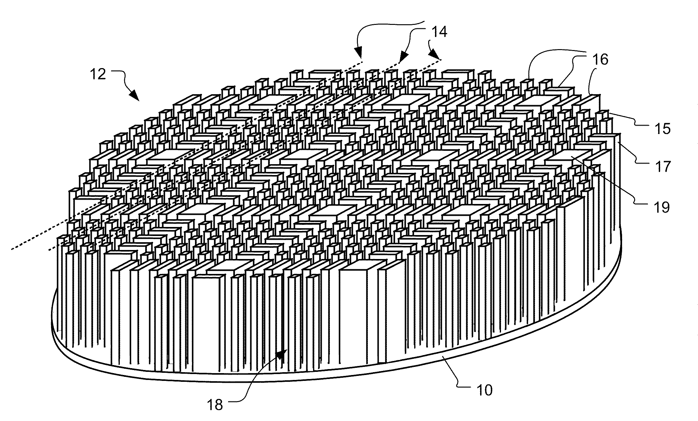
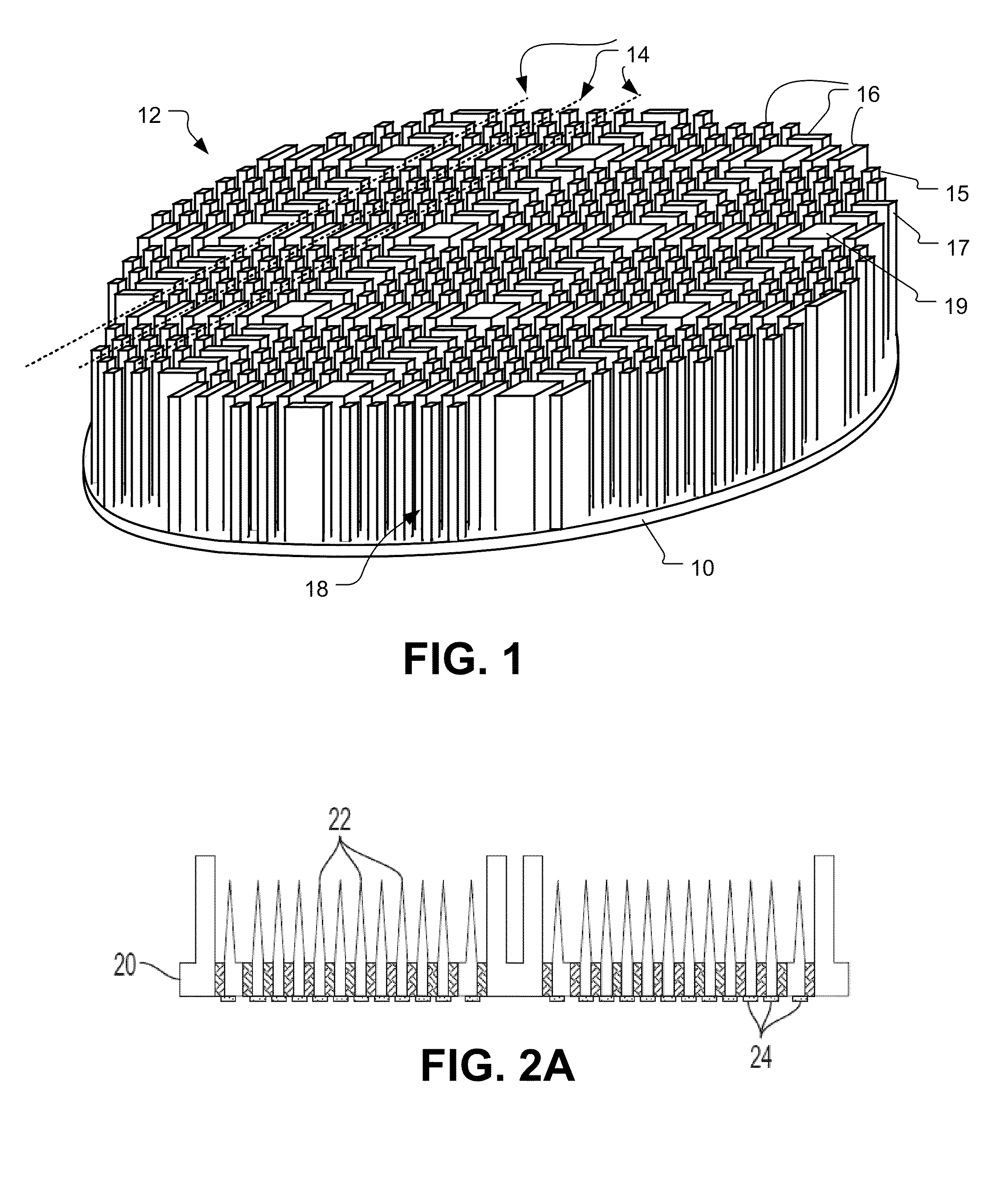
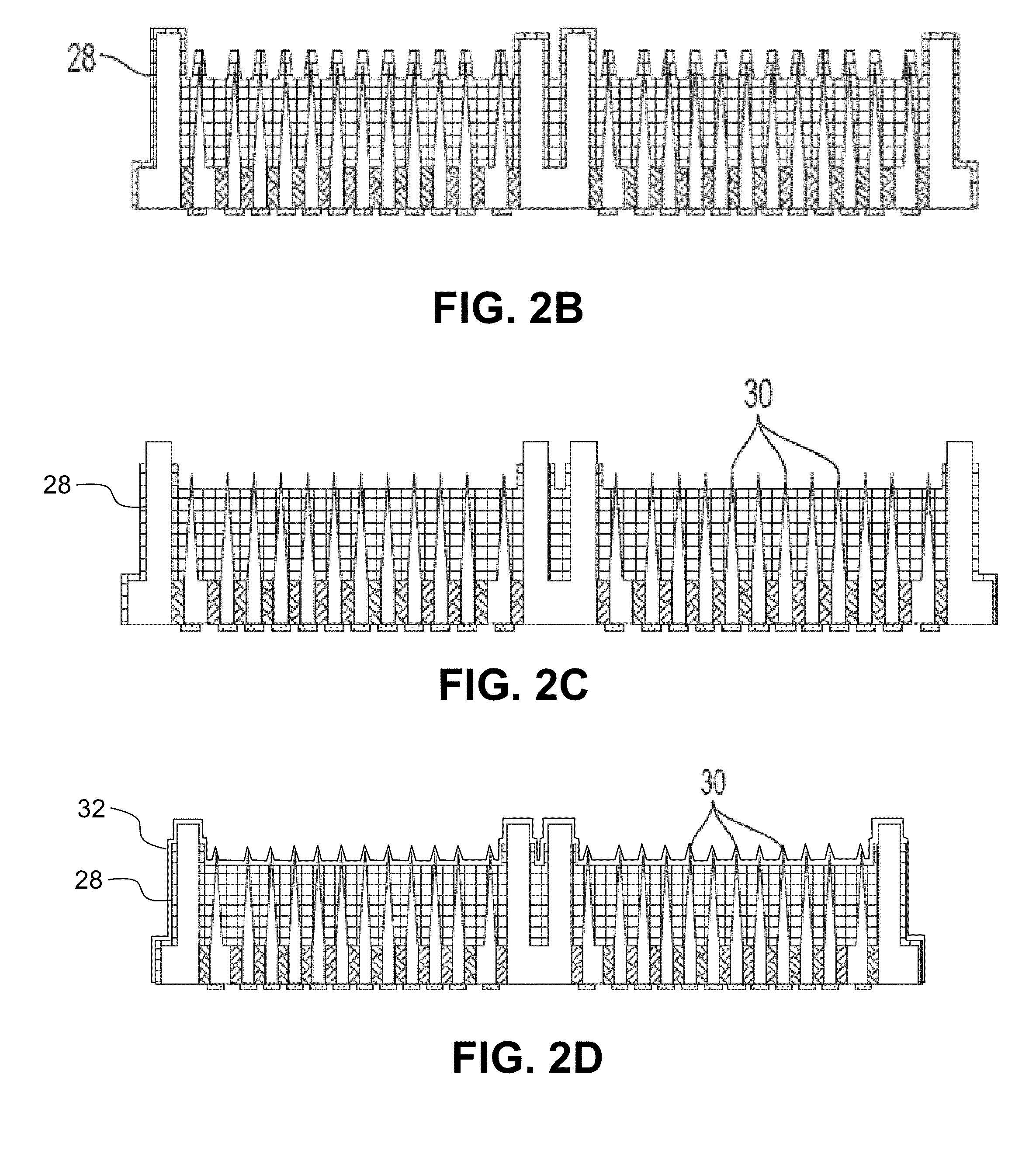
Image

Examples
Embodiment Construction
[0021]In describing embodiments of the present invention, the following terminology will be used.
[0022]The singular forms “a,”“an,” and “the” include plural referents unless the context clearly dictates otherwise. Thus, for example, reference to “a needle” includes reference to one or more of such needles and “etching” includes one or more of such steps.
[0023]As used herein, a plurality of items, structural elements, compositional elements, and / or materials may be presented in a common list for convenience. However, these lists should be construed as though each member of the list is individually identified as a separate and unique member. Thus, no individual member of such list should be construed as a de facto equivalent of any other member of the same list solely based on their presentation in a common group without indications to the contrary.
[0024]Concentrations, amounts, and other numerical data may be expressed or presented herein in a range format. It is to be understood tha...
PUM
| Property | Measurement | Unit |
|---|---|---|
| Fraction | aaaaa | aaaaa |
| Angular velocity | aaaaa | aaaaa |
| Angular velocity | aaaaa | aaaaa |
Abstract
Description
Claims
Application Information